


AI Mentor
Check Your IQ
Free Expert Demo
Try Test
Courses
Dropper NEET CourseDropper JEE CourseClass - 12 NEET CourseClass - 12 JEE CourseClass - 11 NEET CourseClass - 11 JEE CourseClass - 10 Foundation NEET CourseClass - 10 Foundation JEE CourseClass - 10 CBSE CourseClass - 9 Foundation NEET CourseClass - 9 Foundation JEE CourseClass -9 CBSE CourseClass - 8 CBSE CourseClass - 7 CBSE CourseClass - 6 CBSE Course
Offline Centres
Q.
Your Exam Success, Personally Taken Care Of
1:1 expert mentors customize learning to your strength and weaknesses – so you score higher in school , IIT JEE and NEET entrance exams.
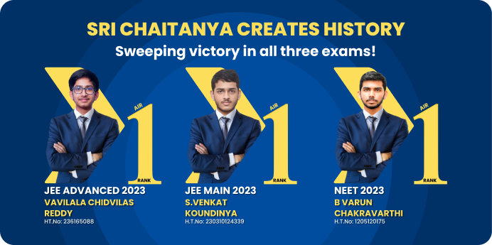
An Intiative by Sri Chaitanya
a
is 0
b
is 1
c
fluctuates between 0 and 1
d
is indeterminate as the circuit can't be realised
answer is A.
(Unlock A.I Detailed Solution for FREE)
Best Courses for You

JEE

NEET

Foundation JEE

Foundation NEET

CBSE
Detailed Solution
Watch 3-min video & get full concept clarity


courses
No courses found
Get Expert Academic Guidance – Connect with a Counselor Today!
best study material, now at your finger tips!

live classes
progress tracking
24x7 mentored guidance
study plan analysis
download the app


Download the App
