

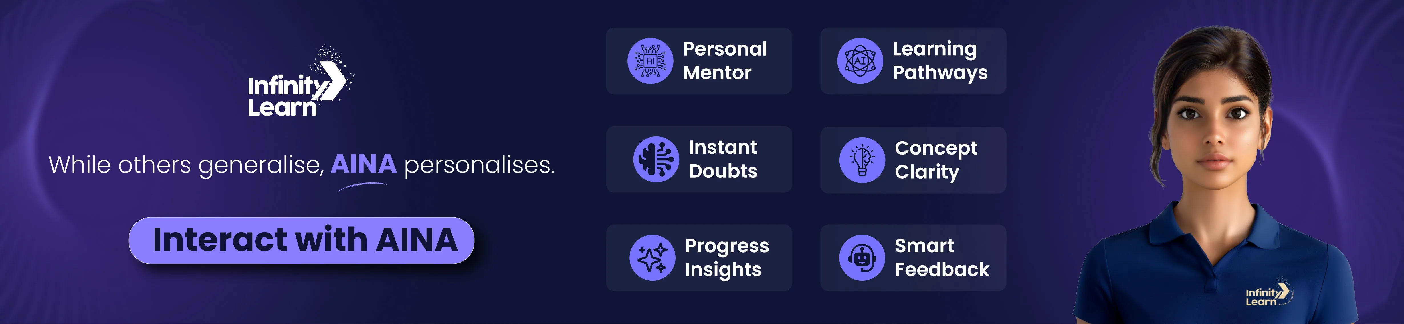

AI Mentor
Check Your IQ
Free Expert Demo
Try Test
Courses
Dropper NEET CourseDropper JEE CourseClass - 12 NEET CourseClass - 12 JEE CourseClass - 11 NEET CourseClass - 11 JEE CourseClass - 10 Foundation NEET CourseClass - 10 Foundation JEE CourseClass - 10 CBSE CourseClass - 9 Foundation NEET CourseClass - 9 Foundation JEE CourseClass -9 CBSE CourseClass - 8 CBSE CourseClass - 7 CBSE CourseClass - 6 CBSE Course
Offline Centres
Q.
Your Exam Success, Personally Taken Care Of
1:1 expert mentors customize learning to your strength and weaknesses – so you score higher in school , IIT JEE and NEET entrance exams.
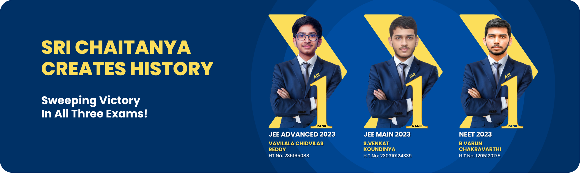
An Intiative by Sri Chaitanya
(Unlock A.I Detailed Solution for FREE)
Best Courses for You

JEE

NEET

Foundation JEE

Foundation NEET

CBSE
Detailed Solution
Watch 3-min video & get full concept clarity

courses
No courses found
Get Expert Academic Guidance – Connect with a Counselor Today!
best study material, now at your finger tips!

live classes
progress tracking
24x7 mentored guidance
study plan analysis
download the app


Download the App
