Table of Contents
Introduction: Forward & Reverse Bias
Prior to actually comparing the two types of bias, it is better to check their individual characteristics. Bias, as well known as biassing, is really a method of establishing a set of currents or voltages at various points of an electronic circuit in order to establish proper operating conditions within an electronic component. Moreover, there are two types of biassing: forward bias and reverse bias. A diode (PN junction) is similar to a one-way highway in that it allows current to flow more easily in one direction than the other. In brief, a diode typically conducts current in only one direction, and the voltage applied follows a predefined forward biassing orientation. When the voltage moves in the opposite direction, this is referred to as reverse bias. In addition, when reversing biased, a standard PN junction diode will typically inhibit or block the flow of current, acting almost like an electronic check valve.
Overview
Forward biassing happens in a standard diode when the voltage across the diode allows the natural flow of current, whereas reverse biassing denotes a voltage across the diode in the opposite direction. Even so, the voltage applied across a diode during reverse biassing does not result in any significant current flow. Moreover, this property is advantageous when converting alternating current (AC) to direct current (DC) (DC). This property has a variety of other applications, including electronic signal control.
An external voltage is applied across the PN-junction diode during forwarding biassing. Such a voltage cancels the potential barrier and creates a low resistance path for current flow. The forward bias indicates that the positive region is connected to the supply’s p-terminal and the negative region is connected to the device’s n-type.
The negative region is connected to the positive terminal of the battery and the positive region is connected to the negative terminal in reversed bias. The potential barrier’s strength is increased by the reverse potential. The potential barrier prevents charge carriers from flowing across the junction. This generates a high resistive path through which no current flows in the circuit.
Forward Biased PN Junction
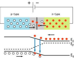
When the p-type region of a PN junction is connected to the positive terminal of a voltage source and the n-type region is connected to the negative terminal of the voltage source, the junction is said to be forward-biased.
Due to the attraction of the positive terminal of the source in this forward-biased condition, electrons that participated in covalent bond formation in the p-type material will be attracted towards the terminal.
As an outcome, covalent bonds are broken and electrons are shifted to the positive terminal. Finally, the concentration of electrons in the crystal closer to the terminal increases, and these electrons recombine with holes here.
As a result, the number of holes increases in the p-type region away from the junction and decreases in the p-type region closer to the terminal as such holes are shifted from terminal to junction.
Because of the higher concentration of holes adjacent to the negative impurity ions layer, the electrons of negative ions escape and recombine with those holes, resulting in the formation of new holes in the layer. As a result, the width of this negative ions layer decreases and eventually vanishes.
Likewise, because of the negative terminal of the source, free electrons in the n-type region will repeal towards the junction, where they will encounter a layer of positive impurity ions and begin recombining with these ions, generating free electrons within the layer. As a result, the width of positive impurity ions decreases and, eventually, vanishes.
Both ion layers will vanish in this manner, and there will be no more depletion layer. Following the removal of the depletion layer, free electrons from the n-type region and holes from the p-type region can easily drift to the n-type region in the crystal.
As a result, ideally, there will be no resistance to current flow, and the PN junction will act as a short circuit.
The total removal of the barrier creates a low resistance path for current flow. As a result, the current begins to flow through the junction. One such current is referred to as forward current.
Reverse Biased PN Junction
If a voltage source’s positive terminal is connected to the n-type region and its negative terminal is connected to the p-type region. When a PN junction is reverse biassed, it is said to be in reverse bias mode.
While no voltage is applied across the p n junction, the potential developed across the junction is 0.3 volts at 25oC for germanium and 0.7 volts at 25oC for silicon.
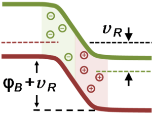
Now, the polarity of such a potential barrier is the same as the polarity of the voltage source used during the reverse biased condition. When the reverse-biased voltage across the PN junction is increased, so is the barrier potential developed across the PN junction. As a result, the PN junction is widened.
Whenever the positive terminal of the source is connected to the n-type region, the free electrons in that region are attracted to the positive terminal of the source, causing more positive impurity ions to be formed in the depletion layer, thickening the layer of positive impurity ions.
Around the same time, electrons are injected in the p-type region of the junction because the negative terminal of the source is connected to it.
Because of the positive potential of the n-type region, electrons are drawn towards the junction, where they combine with holes adjacent to the layer of positive impurity ions to produce more positive impurity ions. So then, the layer’s thickness grows.
As a result, the overall width of the depletion layer grows, as does its barrier potential. This widening of the depletion layer will continue until the barrier potential reaches the reverse-biased voltage applied.
Even though this increase in barrier potential will continue until the applied reverse biased voltage is reached, the depletion layer will disappear due to Zener and avalanche breakdowns if the applied reverse biased voltage is sufficiently high.
It should also be noted that after the reverse-biased depletion layer has been completed, there is no more drift of charge carriers (electrons and holes) through the junction because the potential barrier resists the applied voltage, which has the same value as the potential barrier.
A forward bias really does have a significant forward current, whereas a reverse bias has a negligible forward current. A diode’s depletion layer is significantly thinner in forward bias and much thicker in reverse bias. Forward bias reduces diode resistance, while reverse bias increases diode resistance. Forward bias weakens the potential barrier, allowing current to flow easily across the junction, whereas reverse bias strengthens the potential barrier, obstructing charge carrier flow.

FAQs
Is LED forward biased?
A light-emitting diode (LED) is indeed a semiconductor that emits light. Whenever the LED is forward biased, it emits light; when it is reverse biased, it emits no light. The light intensity has always been proportional to the square of the current flowing through the device.
What are forward bias characteristics?
Within the junction diode, current flows by both majority carriers; however, current flows by electrons only in an external circuit. The flow of current in forwarding bias is of the order of mA. When the applied voltage is increased, the temperature rises as well.
Is photodiode reverse biased?
To operate in the photoconductive mode, the photodiode is reverse biased. The width of the depletion layer grows as the photodiode is biased in reverse. This reduces junction capacitance and, as a result, response time. In impact, the reverse bias causes the photodiode to respond faster.


