Table of Contents
William Shockley, in 1951 invented the primary junction transistor with again to again p-n junctions. Over the years, many kinds of transistors have been invented and differentiated junction transistors from the brand new ones, we name them Bipolar Junction Transistors.
A Bipolar Junction Transistor (BJT) is a 3-terminal semiconductor tool that includes p-n junctions and is capable of amplifying or enlarging a signal. A BJT is a current-controlled tool. A bipolar junction transistor has 3 terminals: emitter, base and collector. A junction transistor makes use of each electron and holes as rate carriers.
Working of Junction Transistor
In comparison to the emitter and collector, the bottom of an electronic transistor is formed thin and is gently doped which implies that the density of the bulk carriers within the base is smaller amount than the density of majority carriers in the emitter and collector.
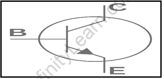
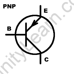
The flow of current is provided through the emitter and also the collector collects them. For a correct connection between the emitter and the collector, the base provides the interaction for the connectivity. In a very junction transistor, the arrow points towards the conventional current. within the n-p-n transistor’s emitter, the arrow points far from the base, and in a very p-n-p transistor’s emitter, the arrow points towards the base. The base-emitter junction is typically forward biassed and also the base-collector junction is reversed biassed once the junction transistor is employed in a circuit.
Two Types of Bipolar Junction Transistors
Junction transistors fall into two categories:
- NPN transistor
- PNP transistor
In an n-p-n junction transistor, p-type carriers have the majority, while n-type carriers dominate at the other ends. In a p-n-p transistor, on the other hand, the minority carriers are n-type while the majority carriers are p-type.
NPN transistor

In an NPN transistor, a p-type semiconductor base is sandwiched between an n-doped emitter and an n-doped collector. NPN transistors are the best used bipolar transistors because of the benefit of electron mobility over electron-hole mobility.
The figure shows the development and symbol of NPN transistors. The bulk charge carriers in an n-p-n transistor are electrons and holes are the minority charge carriers. A little quantity of current at the bottom terminal causes an oversized amount of current to result from emitter to collector. Because of the forward biassing of the transistor, the majority of charge carriers in the emitter are repelled towards the bottom. The electron-hole recombination at the base is extremely little within the base region and most of the electrons cross into the collector region.
PNP transistor

An n-type semiconductor base is sandwiched between a p-doped emitter and a p-doped collector in a PNP transistor. A transistor of this type is characterized by a majority of holes and a minority of electrons. With a PNP transistor, the emitter is forward biassed and the collector is reverse biassed.
Bipolar Junction Transistor
A bipolar junction transistor could be a 3-terminal semiconductor device that consists of 2 p-n junctions that are able to amplify or enlarge a signal. it’s a current controlled device. The three terminals of the BJT are the bottom, the collector, and also the emitter. A symbol of a little amplitude applied to the base is offered within the amplified kind at the collector of the transistor. This can be the amplification provided by the BJT. Note that it will need an external supply of DC power to provide to hold out the amplification process.BJT is a semiconductor device that’s made with 3 doped semiconductor Regions i.e. Base, Collector & emitter separated by two p-n Junctions.
Bipolar transistors are manufactured in two types, PNP and NPN, and are offered as separate components, typically in giant quantities. The prime use or operation of this kind of transistor is to amplify current. This makes them helpful as switches or amplifiers. They need a good application in electronic devices like mobile phones, televisions, radio transmitters, and industrial control.
Operation of Bipolar Junction Transistor
Bipolar junction transistors have three operating regions:
- Transistor active region: Area where transistors work as amplifiers.
- It is the region of the transistor where the collector current reaches the saturation current when the transistor is fully on.
- The transistor is fully off when the collector current is zero in the cut-off region.
Types of Bipolar Junction Transistor
In a bipolar junction transistor, there are two types:
- Bipolar transistor with PNP junction
- Transistor with NPN bipolar junction
PNP BJT
In PNP BJT, the n-type semiconductor is sandwiched among the 2 p-type semiconductors. The p-type semiconductors act as emitter and collector respectively at the same time as the n-type semiconductor acts as a base. This is proven withinside the figure below.
The current enters the transistor via the emitter such that the emitter-base junction is forward biassed and the collector-base junction is opposite biassed.
NPN BJT
An NPN BJT, a p-type semiconductor, is sandwiched among the 2 n-type semiconductors. The n-type semiconductors act as emitter and collector respectively whilst the p-type semiconductor acts as a base. This is proven withinside the figure below.
Current getting into the emitter, base, and collector has the signal convention of positive whilst the current that leaves the transistor has the signal convention of negative.
Also read: Conductors and Insulators
FAQs
Why is there a maximum limit for the collector supply voltage for a transistor?
The maximum collector current for a transistor can be increased rapidly without damaging it because there is a limit to the voltage at which the collector current can be supplied. A maximum voltage should be set in the collector in order to prevent this.
Q. What happens if the transistor is not biassed properly?
Ans: The following list illustrates the consequences of improper passing of a transistor:
- The transistor’s work efficiency decreases
- Distortion will be present in the output signal
- It is possible for the operating point to shift


