
Table of Contents
8085 Pin Diagram: In the realm of digital electronics, microprocessors have transformed our understanding of computing. Among the early trailblazers, the 8085 microprocessor is a significant milestone that ushered in a new era. Known for its versatility and efficiency, the 8085 was crucial in the evolution of early computer systems.
At its heart, the 8085 microprocessor acts as a powerful integrated circuit, functioning as the central processing unit of a computer. It manages instruction execution and controls various components. Grasping its pin diagram is essential for anyone who wants to understand how this remarkable technology works internally.
8085 Microprocessor


The 8085 microprocessor, developed by Intel in the mid-1970s, stands as a cornerstone in the history of computing. Even with the advent of advanced microprocessors, the 8085 remains an excellent educational tool due to its simplicity and effectiveness. In this blog, we will delve into the architecture of the 8085 microprocessor, explore its primary functions, and provide a detailed explanation of its 40-pin configuration.
Also Check: Block Diagram of Computer
Pin Diagram of 8085 Microprocessor


Architecture of 8085 Microprocessor
The 8085 microprocessor is an 8-bit microprocessor, which means it processes 8 bits of data simultaneously. It has a robust and efficient architecture comprising various components:
Arithmetic and Logic Unit (ALU): The ALU performs arithmetic operations like addition, subtraction, increment, and decrement, and logic operations like AND, OR, NOT, and XOR.
Accumulator: This is an 8-bit register that holds one of the operands of an arithmetic or logic operation and stores the result.
Registers: The 8085 has six 8-bit general-purpose registers (B, C, D, E, H, L) which can be paired as BC, DE, and HL to perform 16-bit operations. It also includes a 16-bit stack pointer and a 16-bit program counter.
Instruction Register and Decoder: The instruction register temporarily holds the current instruction fetched from memory, while the decoder interprets this instruction and determines the subsequent operation.
Timing and Control Unit: This unit generates the necessary control signals to synchronize the operations of the microprocessor.
Interrupt Control: The 8085 microprocessor can be interrupted by external events, and the interrupt control manages these signals.
Serial I/O Control: This controls the serial data communication by converting parallel data to serial form and vice versa.
Functions of the 8085 Microprocessor
The 8085 microprocessor performs several key functions that make it versatile for various applications:
- Data Transfer: Moving data between registers, memory, and I/O ports.
- Arithmetic Operations: Executing operations such as addition, subtraction, increment, and decrement.
- Logical Operations: Performing logical operations like AND, OR, XOR, and compare.
- Branching: Directing the flow of execution through jumps, calls, returns, and conditional branches.
- Control Operations: Managing control tasks like interrupt handling, machine control, and status reporting.
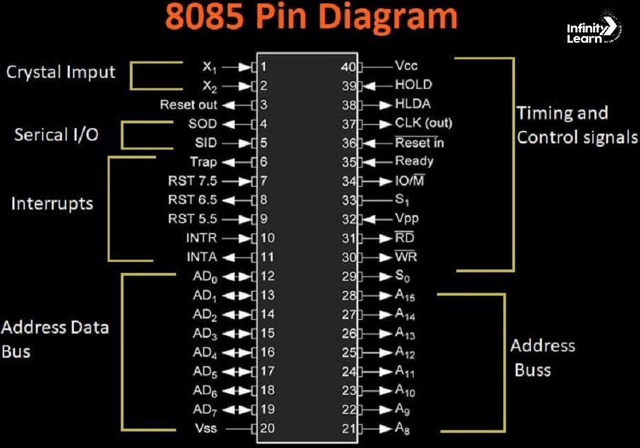
Detailed Pin Description of 8085 Microprocessor
The 8085 microprocessor comes in a 40-pin dual in-line package (DIP). Lets have a look at detailed description of each pin:
- A8-A15 (Pins 21-28): These are higher-order address bus lines, which are used to address memory locations.
- AD0-AD7 (Pins 12-19): These lines serve a dual purpose as lower-order address and data bus. They carry address bits during the first clock cycle (T1) and data bits during the subsequent cycles (T2, T3, Tw, T4) due to time-multiplexing..
- ALE (Pin 30): The Address Latch Enable pin is used to demultiplex the address-data lines. ALE is high during the T1 cycle to latch the address into the address latch.
- IO/M (Pin 31): This pin distinguishes whether the operation is a memory operation (IO/M = 0) or an I/O operation (IO/M = 1).
- S1 and S0 (Pins 29 and 33): These status pins indicate the type of operation being performed. The combination of these signals can represent various machine cycles such as opcode fetch, memory read/write, I/O read/write, etc.
- RD (Pin 32): Read control signal. When RD is low, it indicates that the microprocessor is reading data from memory or an I/O device.
- WR (Pin 31): Write control signal. When WR is low, it indicates that the microprocessor is writing data to memory or an I/O device.
- READY (Pin 35): This pin is used to delay the microprocessor’s read or write cycles until a slow-responding peripheral is ready to communicate.
- HOLD (Pin 39) and HLDA (Pin 38): HOLD indicates that another master is requesting the use of the address and data bus. When the 8085 receives the HOLD signal, it acknowledges via the HLDA signal.
- INTR (Pin 10) and INTA (Pin 11): INTR is a general-purpose interrupt, while INTA is the interrupt acknowledgment.
- RST7.5, RST6.5, and RST5.5 (Pins 7, 8, 9): These are restart interrupts. They can be used to call specific memory locations.
- TRAP (Pin 6): This is a non-maskable interrupt and has the highest priority.
- RESET IN (Pin 36) and RESET OUT (Pin 3): RESET IN initializes the microprocessor by resetting the program counter to zero. RESET OUT indicates that the microprocessor is being reset.
- CLK OUT (Pin 37): This pin provides the system clock for peripheral devices.
- X1 and X2 (Pins 1 and 2): These pins connect to an external crystal oscillator to generate the clock signal.
- VCC (Pin 40) and VSS (Pin 20): VCC is the power supply (+5V), and VSS is the ground.
Also Check: History of Computers


Addressing Modes in the 8085 Microprocessor
The 8085 microprocessor employs several addressing modes to specify the location of data or instructions during program execution. These modes provide flexibility in how operands are accessed and manipulated, enhancing the efficiency of program execution.
Here are some detailed addressing modes in the 8085 microprocessor:
- Immediate Addressing Mode:
In this mode, the operand is included directly within the instruction itself. - Register Addressing Mode:
Here, the operand is located in one of the microprocessor’s registers. - Direct Addressing Mode:
In this mode, the instruction directly specifies the memory address where the operand is located. - Indirect Addressing Mode:
The operand is specified indirectly through a register pair, typically HL. The contents of this register pair serve as the memory address. - Register Indirect with Displacement Addressing Mode:
The operand is determined by adding an 8-bit signed displacement value to the contents of a register pair. This sum is then used as the memory address. - Immediate Indirect Addressing Mode:
In this mode, an immediate value is added to the program counter (PC). The resulting sum is used as the memory address for the operand.
These addressing modes enhance the microprocessor’s ability to handle data and instructions efficiently, making programming more versatile and powerful.
Conclusion
Understanding the pin configuration of the 8085 microprocessor is essential for designing and troubleshooting microprocessor-based systems. Each pin has a specific role, contributing to the overall functionality and efficiency of the microprocessor. The 8085 microprocessor, with its well-defined architecture and versatile pin functionalities, continues to be an important educational tool for learning the basics of microprocessor technology. Whether you’re a student, educator, or hobbyist, grasping the intricacies of the 8085’s pin diagram will undoubtedly enhance your comprehension of microprocessor operations.
Also Refer
ed Questions on 8085 Microprocessor
What is the pin diagram of the 8085 microprocessor?
The pin diagram of the 8085 microprocessor is a visual representation of its physical layout and pin configuration. It shows the placement and function of each of the 40 pins. Key pins include power supply pins (VCC and GND), control and status signals (like RD, WR, and ALE), address and data buses (AD0-AD7 and A8-A15), and interrupt signals (INTR, RST7.5, RST6.5, RST5.5, TRAP).
How many pins are in an 8085 microprocessor?
The 8085 microprocessor has 40 pins.
What is the function of the ALE pin in 8085?
The ALE (Address Latch Enable) pin in the 8085 microprocessor is used to indicate when the multiplexed address/data bus contains an address. It goes high during the first clock cycle to latch the address, and then goes low to allow the bus to be used for data transfer.
What are the blocks of the 8085 microprocessor?
The main blocks of the 8085 microprocessor include: Arithmetic and Logic Unit (ALU): Performs arithmetic and logical operations. Registers: General-purpose registers (B, C, D, E, H, L), accumulator, stack pointer, and program counter. Control Unit: The Control Unit serves as the central coordinator within the microprocessor, overseeing and harmonizing its various operations and functions.. Interrupt Control: Handles the interrupt requests. Timing and Control Circuitry: Generates the necessary control and timing signals. Serial I/O Control: Manages serial input and output operations. Address and Data Buses: Used for communication with memory and I/O devices.
What is the microprocessor 8085 pin diagram?
The pin diagram of the 8085 microprocessor illustrates the functions and locations of all 40 pins. Each pin has a specific role: Power Supply Pins: VCC (power supply) and GND (ground). Address and Data Buses: AD0-AD7 (multiplexed address/data bus) and A8-A15 (address bus). Control and Status Signals: RD (Read), WR (Write), ALE (Address Latch Enable), IO/M (distinguishes between I/O and memory operations). Interrupt Signals: INTR (Interrupt Request), RST7.5, RST6.5, RST5.5 (restart interrupts), TRAP (non-maskable interrupt). Other Pins: RESET IN, RESET OUT (reset signals), CLK OUT (clock output), SID (serial input data), SOD (serial output data). These descriptions help to understand the functionalities and purposes of each pin in the 8085 microprocessor.