Table of Contents
Introduction
A diode is a two-terminal electronic component that conducts current primarily in one direction (asymmetric conductance); it has low resistance (ideally zero) in one direction and high resistance (ideally infinite) in the other. A diode vacuum tube, also known as a thermionic diode, is a vacuum tube with two electrodes, a heated cathode, and a plate, through which electrons can only flow in one direction, from cathode to plate. The most common type today is a semiconductor diode, which is a crystalline piece of semiconductor material with a p–n junction connected to two electrical terminals. Semiconductor diodes were the earliest semiconductor electronic devices. Ferdinand Braun, a German physicist, discovered asymmetric electrical conduction across the contact between a crystalline mineral and a metal in 1874. Today, silicon is used in the majority of diodes, but other semiconducting materials such as gallium arsenide and germanium are also used. A diode’s most common function is to allow an electric current to flow in one direction (referred to as the diode’s forward direction) while blocking it in the opposite direction (the reverse direction). As such, the diode can be thought of as an electronic check valve. This one-way behavior is known as rectification, and it is used to convert alternating current (ac) to direct current (dc) (dc). Diodes, which are rectifier types, can be used in radio receivers to extract modulation from radio signals.
Because of their nonlinear current-voltage characteristics, diodes can have more complicated behavior than this simple on-off action. Semiconductor diodes only begin to conduct electricity when a certain threshold voltage or cut-in voltage is present in the forward direction (a state in which the diode is said to be forward-biased). The voltage drop across a forward-biased diode varies only slightly with current and is temperature-dependent; this effect can be used as both a temperature sensor and a voltage reference. Furthermore, when the reverse voltage across the diode reaches a value known as the breakdown voltage, the diode’s high resistance to current flowing in the reverse direction abruptly drops too low resistance.
Overview
As the name implies, a semiconductor is an element with partial conducting ability. A semiconductor isn’t a conductor or an insulator. For the best results, some impurities are always added to the semiconductor. This is commonly referred to as doping. Semiconductors are further classified into two types based on the type of impurity: a) p-type semiconductor (positively charged) and b) n-type semiconductor (negatively charged) (negatively charged). When used in isolation, P and N-type semiconductors have limited applications. A p-n junction, on the other hand, is a collaborative use for both p and n-type semiconductors. When a p-n junction is connected to an external voltage source, such as a battery, the entire assembly is referred to as a Semiconductor Diode. Despite the fact that the entire setup is bi- terminal, the current flow is unidirectional.
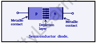
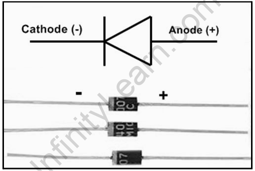
Semiconductor diodes are diodes that are made of semiconducting materials (typically, the metals silicon and germanium are used in them). The negatively charged cathode in these diodes contains a large number of electrons and is placed adjacent to the anode, which contains an excess of positively charged holes. The p-n junction diode and the Zener diode are two common types of semiconductor diodes. In a semiconductor diode, the junction between the cathode and the anode forms a depletion region that is devoid of electrons and holes. When positive voltages are present at the anode, the depletion region shrinks dramatically and current begins to flow through the semiconductor diode.
Semiconductor diode – I-V
Semiconductor devices such as diodes, transistors, and thyristors are all built with connected semiconductor PN junctions, and their I-V characteristics curves will reflect the operation of these PN junctions. In this case, the I-V characteristics of these devices will be non-linear, as opposed to resistors, which have a linear relationship between current and voltage. A semiconductor diode’s primary function, for example, is the rectification of AC to DC. When a diode is forward biased (the higher potential is connected to the Anode), current flows through it. The current is blocked when the diode is reverse biased (the higher potential is connected to the Cathode). For current to flow, a PN junction requires a bias voltage of a specific polarity and amplitude. This bias voltage also controls the resistance of the junction and, as a result, the current flows through it. Take a look at the diode circuit below.
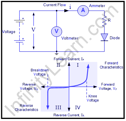
When the diode is forward biassed, or anode positive in relation to the cathode, a forward or positive current flows through it and operates in the top right quadrant of its I-V characteristics curves, as shown. The curve gradually increases into the forward quadrant from the zero intersection, but the forward current and voltage are extremely small.
Characteristics of semiconductor diode
In the case of Semiconductor Diode forward bias and Semiconductor Diode reverse bias, there is a graphical depiction of the voltage and current. When the forward bias is raised, the current increases linearly until it reaches a stable value called the knee voltage. However, after this voltage, the current varies non-linearly. Reverse current is independent of reverse bias, as we all know. Rather, the temperature of the connection determines the current. For every 1-degree increase in temperature, the current multiplies by 7%, according to calculations.
It has the property of only allowing current to flow in one direction. If no voltage is provided across the junction, electrons will diffuse to the p-side and holes will diffuse to the n-side, where they will merge. At absolute zero, semiconductors are perfect insulators. However, because the density of electrons in the conduction band is lower at room temperature than in metals, they cannot conduct current as well as metals. Semiconductors’ electrical conductivity is not as high as that of metals, but it is also not as low as that of insulators.
VI characteristics of p-n junction diode
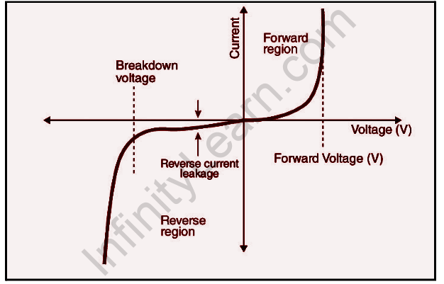
The V-I characteristics of p-n junction diodes are defined by a curve between the voltage and current across the circuit. Voltage is represented on the x-axis, while current is represented on the y-axis. The p-n junction diode’s V-I characteristics curve is depicted in the graph above. We can observe that the diode functions in three separate places with the help of the curve:
- There is no bias.
- Bias toward the future
- Bias in the opposite direction
When the p-n junction diode is at zero bias, no external voltage is applied, implying that the potential barrier at the junction inhibits the current flow. The p-type is connected to the positive terminal of the external voltage, while the n-type is connected to the negative terminal when the p-n junction diode is in forwarding bias. When the diode is put in this manner, the potential barrier is decreased. The potential barriers decrease and current flows when the voltage is 0.7 V for silicon diodes and 0.3 V for germanium diodes.
While the diode is under forwarding bias, the current grows slowly, and the curve formed is non-linear as the voltage applied to the diode overcomes the potential barrier. Once the diode has crossed the potential barrier, it operates normally, and the curve rises rapidly like the external voltage rises, resulting in a linear curve. When the PN junction diode is biased negatively, the p-type is connected to the external voltage’s negative terminal, while the n-type is connected to the positive terminal. As a result, the potential barrier rises. Because there are minority carriers at the junction, reverse saturation current occurs at first.
P-N junction diode
A p-n junction is an interface or border between two types of semiconductor material inside a semiconductor, namely the p-type and the n-type. A semiconductor’s p-side, or positive side, has more holes than the n-side, or negative side, which has more electrons. The p-n junction in a semiconductor is created through the doping process. When we use different semiconductor materials to form a p-n junction, there will be a grain boundary that prevents electrons from moving from one side to the other by scattering electrons and holes, which is why we use doping.
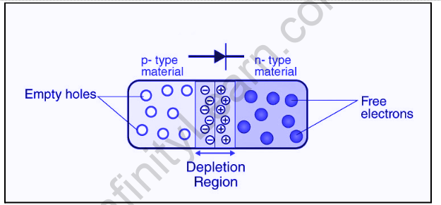
When an electron diffuses from the n-side to the p-side, it leaves a stationary ionized donor on the n-side. As the process progresses, a layer of positive charge forms on the n-side of the junction. When a hole is moved from the p-side to the n-side, an ionized acceptor is left on the p-side, resulting in the formation of a layer of negative charges on the p-side of the junction. The depletion area is defined as a positive and negative charge region on either side of the junction. Because of the positive space charge area on each side of the junction, an electric field direction from a positive charge to a negative charge is generated.
When the p-n junction diode is at zero bias, no external voltage is applied to it.
Forward bias: The p-type is connected to the voltage potential’s positive terminal, while the n-type is connected to the negative terminal.
Reverse bias: The p-type is connected to the voltage potential’s negative terminal, while the n-type is connected to the positive terminal.
A semiconductor material’s electrical conductivity lies between that of a conductor, such as metallic copper, and that of an insulator, such as glass. Its resistivity decreases with increasing temperature, whereas metals have the opposite effect. The conductivity of a crystal structure can be improved by introducing impurities (doping) into it. When two distinct doped areas occur in the same crystal, a semiconductor junction is formed. The behavior of charge carriers such as electrons, ions, and electron holes at these junctions is the foundation of diodes, transistors, and most modern electronics.
Also read: Important Topic Of Physics: Nuclear Fission and Fusion
FAQs – Frequently Asked Questions
What are the various types of diodes?
There are various Diodes, each of which serves a specific purpose. Light Emitting Diode (LED), avalanche diode, laser diode, Schottky diode, Zener diode, PN junction diode, and other types of diodes are available. All of these diodes have different functions; for example, a Light Emitting Diode is used to produce light, whereas a Zener diode is used to regulate voltage.
What exactly is reverse resistance?
Reverse resistance is the resistance supplied by a p-n junction diode when it is reverse biased.
What are the composition and characteristics of a Semiconductor Diode?
Semiconductor diodes are typically made of silicon. In this case, a negatively charged cathode is placed near a positively charged anode. The cathode has an excess of electrons, whereas the anode has an excess of holes (positively charged). Between a cathode and anode, a depletion zone develops in which neither electrons nor holes exist. A diode's characteristics include forward voltage, forward current, reverse voltage, and current.


