NCERT Solutions for Class 12 Physics Chapter 14 - Semiconductor Electronics: Materials, Devices and Simple Circuits
By Ankit Ankit
|
Updated on 28 Oct 2026, 11:53 IST
NCERT Solutions for Class 12 Physics Chapter 14, Semiconductor Electronics: Materials, Devices and Simple Circuits, provide step-by-step answers to the questions given in the NCERT textbook. The chapter introduces the basic principles of semiconductor materials, including energy bands, intrinsic and extrinsic semiconductors, p-type and n-type semiconductors, p-n junctions, and semiconductor diodes.
For the 2026–27 CBSE Physics syllabus, Chapter 14 is part of Unit IX: Electronic Devices. The prescribed content covers energy bands in conductors, semiconductors and insulators, intrinsic and extrinsic semiconductors, p-n junctions, diode I-V characteristics in forward and reverse bias, and the use of a junction diode as a rectifier.
This page provides the exact NCERT exercise questions, followed by detailed solutions with the reasoning and steps needed to reach each answer. It also covers the key concepts, useful relations, important questions from the chapter, and frequently asked questions for revision.
Download Class 12 Physics Chapter 14 NCERT Solutions
Get step-by-step NCERT Solutions for Class 12 Physics Chapter 14, Semiconductor Electronics: Materials, Devices and Simple Circuits, from Infinity Learn. Use the solutions alongside your NCERT textbook to revise energy bands, semiconductor types, p-n junctions, diode characteristics and rectification.
NCERT Class 12 Physics Chapter 14: Structure and Key Topics
Chapter 14 moves from the properties of semiconductor materials to their behaviour in electronic circuits.
Energy Bands
The chapter begins with the classification of solids using electrical conductivity and energy-band concepts. The relative arrangement of the valence band, conduction band and energy gap explains why materials behave as conductors, insulators or semiconductors.
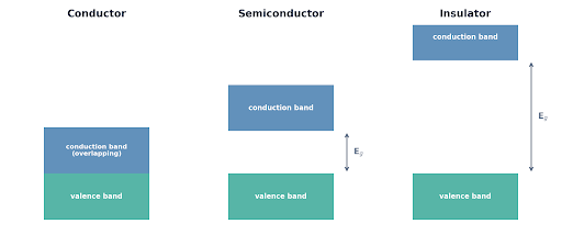
In a conductor the bands overlap; in a semiconductor the gap is small; in an insulator it is large

Intrinsic Semiconductors
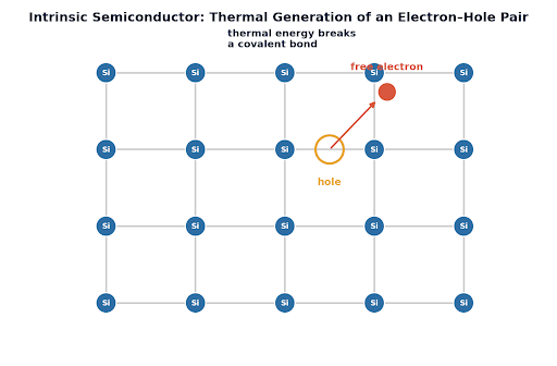
Pure silicon and germanium are introduced as intrinsic semiconductors. Thermal energy can generate electron-hole pairs, allowing both electrons and holes to contribute to electrical conduction.
Best Courses for You

JEE

NEET

Foundation JEE

Foundation NEET

CBSE
Breaking a covalent bond thermally creates one free electron and one hole
Extrinsic Semiconductors
The chapter then explains doping. Adding suitable impurities to silicon or germanium produces n-type or p-type semiconductors. In n-type material, electrons are the majority carriers, while in p-type material, holes are the majority carriers. (See the diagrams under Questions 1 and 2 below.)
p-n Junction
When p-type and n-type regions are joined, charge carriers diffuse across the junction. This leads to the formation of a depletion region and a potential barrier.
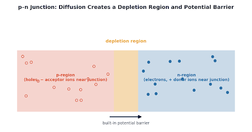
Diffusion of carriers across the junction leaves behind fixed ions, creating the depletion region and barrier
Biasing and Diode Characteristics
The effect of forward and reverse bias on a p-n junction is explained through the diode's current-voltage characteristics.
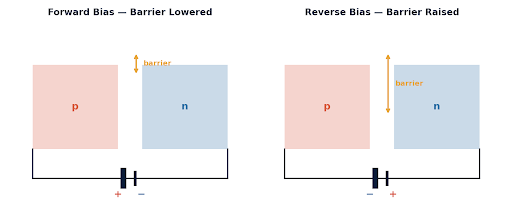
Forward bias opposes and lowers the built-in barrier; reverse bias adds to it and raises the barrier
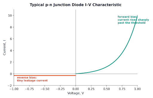
Current rises sharply in forward bias past a threshold voltage, while only a tiny leakage current flows in reverse bias
Rectification
The final part covered here explains how a semiconductor diode can be used for rectification. The NCERT exercise includes a question on the output frequency of half-wave and full-wave rectifiers (see Question 6 below).
Important Formulas for Chapter 14
The following relations are useful while studying the concepts and solving the NCERT exercises:
| Concept | Formula |
| Intrinsic carrier concentration | ne = nh = ni |
| Total current (electron + hole) | I = Ie + Ih |
| Half-wave rectifier output frequency | fout = fin |
| Full-wave rectifier output frequency | fout = 2fin |
Here ne is the electron concentration, nh is the hole concentration and ni is the intrinsic carrier concentration. These relations are directly useful for NCERT Exercise 14.6.
Important Questions
The following questions are the actual NCERT exercise questions, reproduced without changing their wording.
Question 1 — NCERT Exercise 14.1
In an n-type silicon, which of the following statement is true:
(a) Electrons are majority carriers and trivalent atoms are the dopants.
(b) Electrons are minority carriers and pentavalent atoms are the dopants.
(c) Holes are minority carriers and pentavalent atoms are the dopants.
(d) Holes are majority carriers and trivalent atoms are the dopants.
Solution
Silicon has four valence electrons. To form an n-type semiconductor, it is doped with a pentavalent impurity having five valence electrons — the extra electron becomes available for conduction.
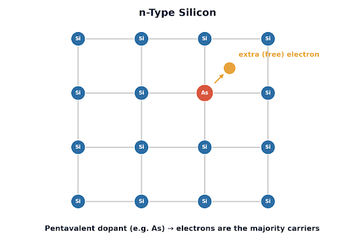
A pentavalent dopant (e.g. arsenic) contributes one extra, loosely-bound electron
Therefore, in n-type silicon, electrons are the majority carriers, holes are the minority carriers, and the dopant is pentavalent. Checking each option against this: (a) and (d) wrongly name a trivalent dopant; (b) wrongly calls electrons the minority carrier. Only (c) correctly pairs “holes are minority carriers” with “pentavalent dopant.”
→ (c) Holes are minority carriers and pentavalent atoms are the dopants.
Question 2 — NCERT Exercise 14.2
Which of the statements given in Exercise 14.1 is true for p-type semiconductors?
Solution
A p-type semiconductor is formed by doping silicon or germanium with a trivalent impurity. A trivalent atom has three valence electrons, whereas silicon has four — this results in a vacancy that behaves as a hole.
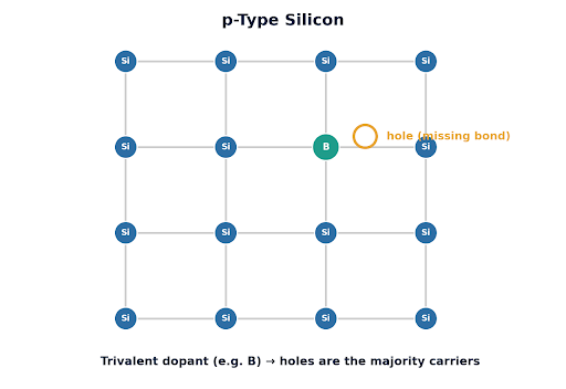
A trivalent dopant (e.g. boron) leaves one bond incomplete — a hole
In a p-type semiconductor, holes are the majority carriers, electrons are the minority carriers, and the dopant is trivalent. From the same four statements in Exercise 14.1, this matches option (d).
→ (d) Holes are majority carriers and trivalent atoms are the dopants.
Question 3 — NCERT Exercise 14.3
Carbon, silicon and germanium have four valence electrons each. These are characterised by valence and conduction bands separated by energy band gaps respectively equal to (Eg)C, (Eg)Si and (Eg)Ge. Which of the following statements is true?
(a) (Eg)Si < (Eg)Ge < (Eg)C
(b) (Eg)C < (Eg)Ge > (Eg)Si
(c) (Eg)C > (Eg)Si > (Eg)Ge
(d) (Eg)C = (Eg)Si = (Eg)Ge
Solution
Carbon, silicon and germanium have the same number of valence electrons, but those valence electrons occupy progressively higher shells moving from carbon to silicon to germanium, which weakens how tightly they are held and shrinks the energy gap.
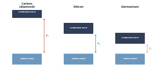
The band gap is largest for carbon (diamond), smaller for silicon, and smallest for germanium
The band gap is therefore largest for carbon, smaller for silicon, and smallest for germanium.
→ (c) (Eg)C > (Eg)Si > (Eg)Ge
Question 4 — NCERT Exercise 14.4
In an unbiased p-n junction, holes diffuse from the p-region to n-region because
(a) free electrons in the n-region attract them.
(b) they move across the junction by the potential difference.
(c) hole concentration in p-region is more as compared to n-region.
(d) All the above.
Solution
In a p-type semiconductor, holes are the majority carriers, so their concentration is much higher in the p-region than in the n-region. Charge carriers naturally diffuse from a region of higher concentration towards a region of lower concentration — this is ordinary diffusion, independent of any electric field or potential difference (which is why (a) and (b) describe drift, not diffusion, and are not the reason for this particular motion).
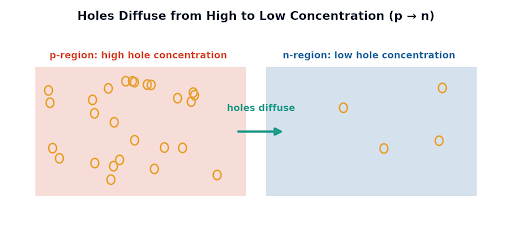
Holes diffuse down their concentration gradient, from the p-region into the n-region
→ (c) hole concentration in p-region is more as compared to n-region.
Question 5 — NCERT Exercise 14.5
When a forward bias is applied to a p-n junction, it
(a) raises the potential barrier.
(b) reduces the majority carrier current to zero.
(c) lowers the potential barrier.
(d) None of the above.
Solution
In forward bias, the p-side of the junction is connected to the positive terminal of the external supply and the n-side to the negative terminal. This applied voltage opposes the junction's built-in potential barrier.
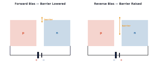
Forward bias (left) opposes the built-in barrier and lowers it; reverse bias (right) adds to it
As a result, the potential barrier decreases, which is what allows majority-carrier current to flow easily under forward bias.
→ (c) lowers the potential barrier.
Question 6 — NCERT Exercise 14.6
In half-wave rectification, what is the output frequency if the input frequency is 50 Hz. What is the output frequency of a full-wave rectifier for the same input frequency.
Solution
Part 1: Half-wave rectifier
In half-wave rectification, only one half-cycle of the input AC signal contributes to the output during each complete input cycle, so:
→ fout = fin = 50 Hz
Part 2: Full-wave rectifier
In full-wave rectification, both half-cycles of the AC input are used, so two output pulses are produced during every complete input cycle:
→ fout = 2fin = 2 × 50 = 100 Hz
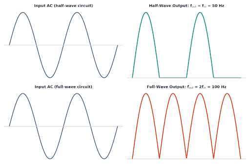
A half-wave rectifier passes one pulse per input cycle; a full-wave rectifier passes two
Therefore, the output frequency is 50 Hz for a half-wave rectifier and 100 Hz for a full-wave rectifier, for a 50 Hz input.
Key Features of NCERT Solutions for Class 12 Physics Chapter 14 Semiconductor Electronics
- Detailed Problem Solutions: Each question is worked out with the reasoning and steps needed to understand the approach used to find the answer.
- Concepts Before Application:Semiconductor concepts are explained clearly before students see how they are used in the questions.
- Clear Use of Formulas: Relevant equations and relations are introduced before they are used in numerical problems.
- Focused on Current CBSE Topics: The solutions cover the semiconductor concepts included in the current Class 12 Physics syllabus.
- Easy to Follow Format: Each problem is presented with its solution, allowing students to try the question first and then compare their working.
Why Infinity Learn NCERT Solutions for Class 12 Physics Chapter 14 Semiconductor Electronics
- Learn from Physics Experts: Get clear explanations of semiconductor topics from experienced Physics faculty.
- Understand with Diagrams: Use simple diagrams to understand p-n junctions, semiconductor devices, and rectifier circuits.
- Prepare for JEE and NEET: Practice relevant competitive-exam questions along with your NCERT preparation.
- Practice After Learning: Use chapter-wise questions and tests to check how well you have understood the concepts.
- Clear Your Doubts: Get help with difficult semiconductor concepts, diagrams, and circuit-based questions.
course
No courses found
FAQs on
What is the difference between a conductor, semiconductor, and insulator?
The main difference lies in their electrical conductivity and energy-band structure. Conductors have very high conductivity and either a partially filled conduction band or overlapping valence and conduction bands. Insulators have a large forbidden energy gap, making the movement of electrons to the conduction band difficult. Semiconductors have a smaller energy gap, allowing some electrons to acquire enough thermal energy to participate in conduction.
How does a p-n junction diode work as a rectifier?
A p-n junction diode allows current to pass readily when it is forward-biased and offers very high resistance under reverse bias, apart from a small reverse current. This one-directional behaviour allows a diode to convert an alternating input into a pulsating direct-current output.
What is the function of a Zener diode?
A Zener diode is a special-purpose diode designed to operate in the reverse breakdown region. However, Zener diodes are not part of the current 2026–27 CBSE Class 12 Physics syllabus content specified for Chapter 14, so this topic is not required for the core syllabus-focused preparation on this page.
Is this chapter important for NEET and JEE Main?
Chapter 14 covers fundamental semiconductor concepts that are relevant to entrance-exam preparation. However, the exact topics and question distribution can vary between examinations and years. Students should use the applicable examination syllabus rather than relying on claims about fixed chapter-wise question frequency.
Where can I download the NCERT Solutions PDF for Chapter 14?
You can access the Class 12 Physics Chapter 14 NCERT Solutions through the resources available on this page. The solutions cover all six NCERT exercise questions from the chapter.
