Table of Contents
Semiconductors are special materials that aren’t quite as good at conducting electricity as metals, but they’re also not as bad as materials like ceramics. They can be made of simple elements like silicon or compounds like gallium arsenide.
Also Check: CBSE syllabus 2024
Semiconductor Electronics Important Questions for CBSE Class 12 Physics Semiconductor, Diode and its Application
Also Check: Geography Class 12 Notes Chapter 9
4.Energy Band In a crystal due to interatomic interaction, valence electrons of one atom are shared by more than one atom in the crystal. Now, splitting of energy level takes place. The collection of these closely spaced energy levels are called an energy band.
5.Valence Band Valence band are the energy band which includes the energy levels of the valence electrons.
6.Conduction Band Conduction band is the energy band above the valence

Also Check: Class 12 Important Questions Political Science

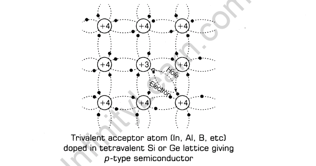



25.Diode as Rectifier The process of converting alternating voltage/current into direct voltage/current is called rectification. Diode is used as a rectifier for converting alternating current/voltage into direct current/voltage.There are two ways of using a diode as a rectifier i.e.
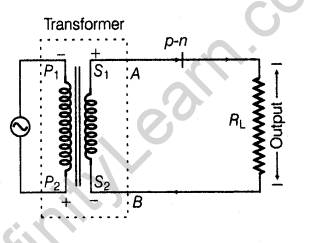
(i)Diode as a Half-Wave Rectifier Diode conducts corresponding to positive half cycle and does not conduct during negative half cycle. Hence, AC is converted by diode into unidirectional pulsating DC. This action is known as half-wave rectification.
Circuit diagram of p-n junction diode as half-wave rectifier is shown below:
The input and output waveforms have been given below
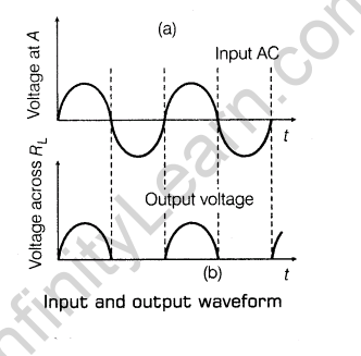
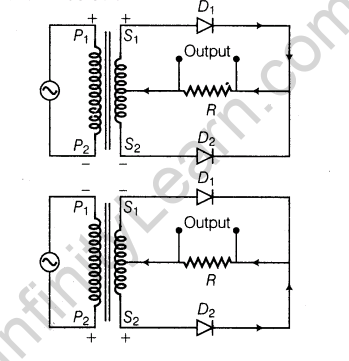
(ii) Diode as a Full-Wave Rectifier In the full-wave rectifier, two p-n junction diodes, D1 and D2 are used. The circuit diagram or full-wave rectifier is shown below:
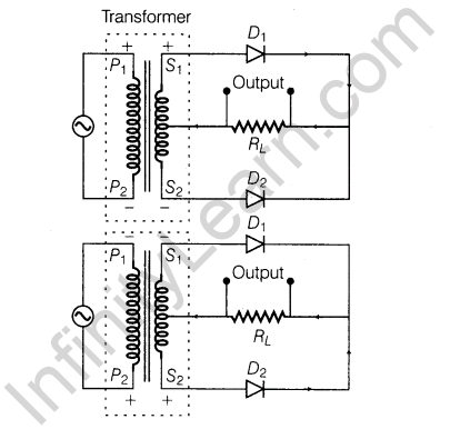
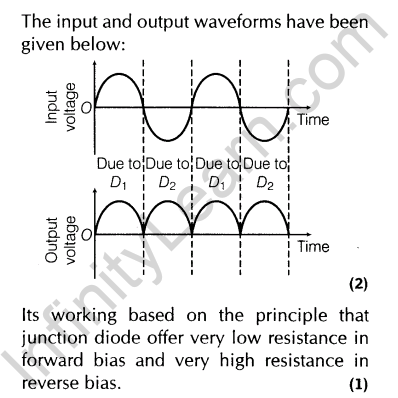
The input and output waveforms have been given below:
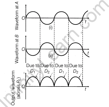

30.Optoelectronic Devices Semiconductor diodes in which carriers are generated by photons, i.e. photo-excitation, such devices are known as optoelectronic devices.
These are as follows:
(i) Light Emitting Diode (LED) It is a heavily doped p-n junction diode which converts electrical energy into light energy.
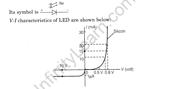
LEDs has the following advantages over conventional incandescent low power lamps
(a)Fast action and no warm up time required
(b)It is nearly monochromatic
(c)Low operational voltage and less power consumed
(d)Fast ON-OFF switching capability.
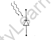
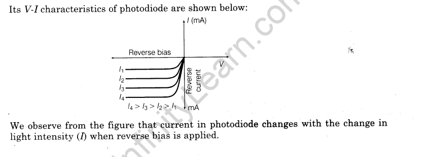
(ii) Photo diode A photodiode is a special type of junction diode used for detecting optical
signals. It is a reverse biased p-n junction made from a photosensitive material.
Its symbol is
Previous Year Examination Questions
1 Mark Questions
1.The graph shown in the figure represents a plot of current versus voltage for a given semiconductor. Identify the region, if any over which the semiconductor has a negative resistance. [All India 2013]
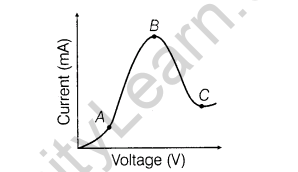
Ans.Resistance of a material can be found out by the slope of the curve V versus I. Part BC of the curve shows the negative resistance as with the increase in current and decrease in voltage.
2.What happens to the width of depletion layer of a p-n junction when it is
(i)forward biased?
(ii)reverse biased? [All India 2011]
Ans.(i) Width of depletion layer’s decreases in forward bias
(ii) Width depletion layer increases in reverse bias.
3.Why cannot we take one slab of p-type semiconductor and physically join it to another slab of n-type semiconductor to get p-n junction?

Ans.In this way, continuous contact cannot be produced at atomic level and junction will behave as a discontinuity for the flowing charge carrier.
4.What is the most common use of photo diode? [All India 2009]
Ans.The photodiode can be used as a photodetector to detect optical signals
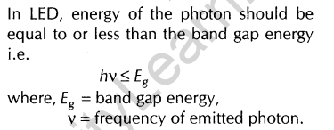
5.State the relation between the frequency v of radiation emitted by LED and the band gap energy E, of the semiconductor used to fabricate it.[All India 2009 C]
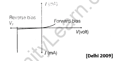
Ans.Zener diode, which is used as a DC voltage regulator.
6.Figure show the I-V characteristics of a given device. Name the device and write where it is used.
Ans.
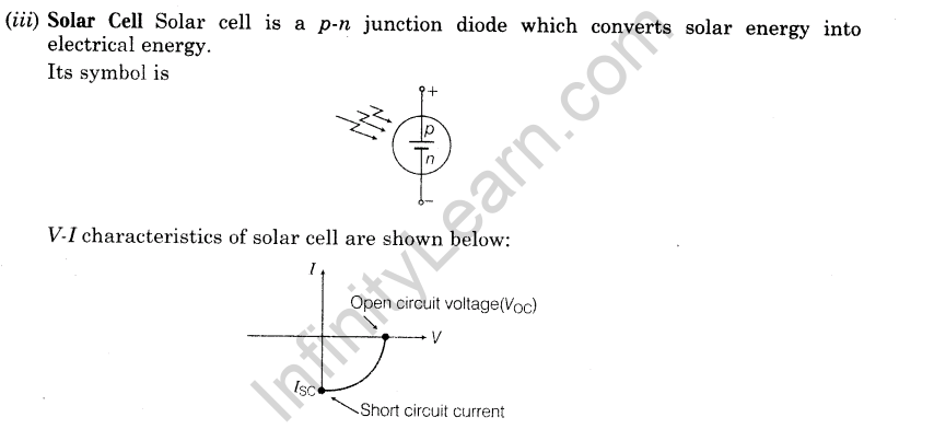
7.State the reason, why GaAs is most commonly used in making of a solar cell. [All India 2008]
Ans.solar radiation is nearly 1.5 eV. In order to have photo excitation, the energy of radiation (hv) must be greater than energy band gap (Eg). Therefore, the semiconductor with energy band gap about 1.5 eV or lower than it and with higher absorption coefficient is likely to give better solar conversion efficiency. The energy band gap for Si is about 1.1 eV, while for GaAs, it is about 1.53 eV. The GaAs is better inspite of its higher band gap than Si because it absorbs relatively more energy from the incident solar radiations being of relatively higher absorption coefficient.
8.At what temperature would an intrinsic semiconductor behave like a perfect insulator? [Delhi 2008 C]
Ans.At O° K temperature, an intrinsic semiconductor behaves like a perfect insulator
9.Why should a photo diode be operated at reverse bias?[All India 2008]
Ans.The photodiodes are used to detect the optical signals. The fraction change in minority carrier in case of reverse biased diode is easily measurable than that of forward biased. That is why photodiode is operated at reverse bias.
2 Marks Questions
10.Explain, with the help of a circuit diagram, the working of a p-n junction diode as a half-wave rectifier. [ah India 2014]
Ans.p-n Junction Diode as a Half-Wave Rectifier AC voltage to be rectified is connected to the primary coil of a step-down transformer. Secondary coil is connected to the diode through resistors Rj,, across which output is obtained.
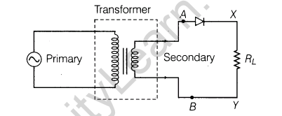
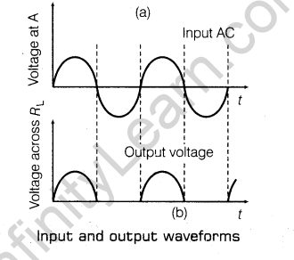
Working During positive half cycle of the input AC, the p-n junction is forward biased. Thus, the resistance in p-n junction becomes low and current flows. Hence, we get output in the load.
During negative half cycle of the input AC, the p-n junction is reverse biased. Thus, the resistance of p-n junction is high and current does not flow. Hence, no output in the load. So, for complete cycle of AC, current flows through the load resistance in the same direction.
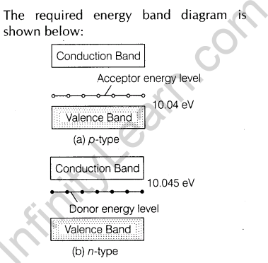
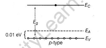
11.Draw energy band diagram of n-type and p-type semiconductor at temperature T > OK. Mark the donar and acceptor energy level with their energies. [Foreign 2014]
Ans.
12.Distinguish between a metal and an insulator on the basis of energy band diagram. [Foreign 2014]
Ans.(i) Metal For metals, the valence band is completely filled and the conduction band can have two possibilities either it is partially filled with an extremely small energy gap between the valence and conduction bands or it is empty, with two bands overlapping each other as shown below:

(ii) On applying an small even electric field, metals can conduct electricity.
(i) Insulators : for insulator, the energy gap between the conduction and valence bands are very large, also the conduction band is practically empty, as shown below:
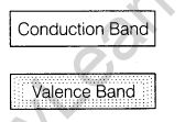
(ii) When an electric field is applied across such a solid, the electrons find it difficult to acquire. So, a large amount of energy is required to reach the conduction band.Thus, the conduction band continues to be empty. That is why no current flows through insulators.
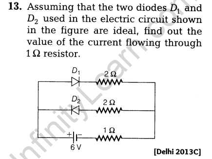
Ans.
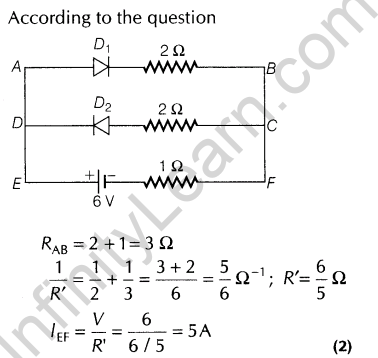
14.Explain the term ‘drift velocity’ of electrons in conductor. Hence, obtain an expression for the current through a conductor in terms of ‘drift velocity’.[All India 2013]
Ans.’Drift velocity’ of electrons in a conductor
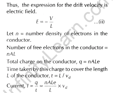
Metals contain a large number of free electrons. These electrons are in continuous random motion. Due to the random motion, the free electrons collide with positive metal ions with high frequency and undergo change in direction at each collision. So, the average velocity for the electrons in a conductor is zero.Now, when this conductor is connected to a source of emf, an electric field is established in the conductor, such that E = V/L
where, V = potential difference across the conductor and L = length of the conductor. The electric field exerts an electrostatic force -Ee on each free electron in the conductor. The acceleration of each electron is given by
![]()
where, e = electric charge on electron and m = mass of electron.
The average velocity of all the free electrons in the conductor is called the drift velocity of free electrons of the conductor.

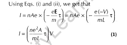
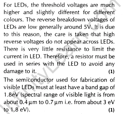
15.Mention the important considerations required while fabricating a p-n junction diode to be used as a Light Emitting Diode (LED). What should be the order of band gap of an LED, if it is required to emit light in the visible range? [Delhi 2013]
Ans.
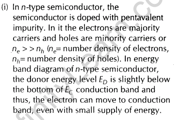
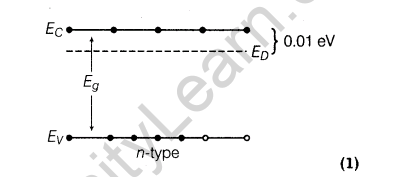
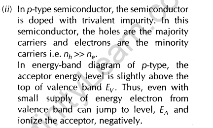
16.Write two characteristics features to distinguish between n-type and p-type semiconductors. [All India 2012]
Ans.
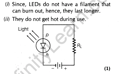
17.Give two advantages of LED’s over the conventional incandescent lamps.[Foreign 2012]
Ans.When we apply sufficient voltage to LED, electron move across the junction into p-region and get attracted to the holes there. Thus, electrons and holes recombine. During each recombination, the electric potential energy is converted into the electromagnetic energy and a photon of light with a characteristic frequency is emitted, this is how, LED works.
Advantages of LEDs over incandescent lamps
(i) Since, LEDs do not have a filament that can burn out, hence, they last longer.
They do not get hot during use.

Ans.When photo diode is illuminated with light due to breaking of covalent bonds, equal number of additional electrons and holes comes into existence whereas fractional change in minority charge carrier is much higher than fractional change in majority charge carrier. Since, the fractional change of minority carrier current is measurable significantly in reverse bias than that of forward bias. Therefore, photo diode are connected in reverse bias.
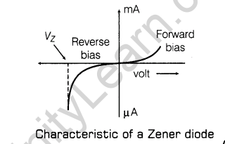
19.Name the semiconductor device that can be used to regulate an unregulated DC power supply. With the help of 7-V characteristics of this device, explain its working principle.[Delhi 2011]
Ans. Zener diode is used as voltage regulator.
Principle Zener diode is operated in the reverse breakdown region. The voltage across it remains constant, equal to the breakdown voltage for large charge in reverse current
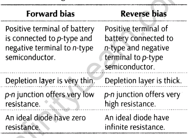
20.How is forward biasing different from reverse biasing in a p-n junction diode? [Delhi 2011]
Ans.Differences between forward and reverse biases are given below:
21.Explain, how a depletion region is formed in a junction diode?[Delhi 2011]
Ans. With the formation of p-n junction, the holes from p-region diffuse into the n-region and electrons from n-region diffuse into p-region and electron-hole pair combine and get annihilated.
This input produces potential barrier, VB across in junction which opposes the further diffusion through the junction. Thus, small region forms in the vicinity of the junction which is depleted of free charge carrier and has only immotile ions is called the depletion region.
22.Draw the circuit diagram showing how a p-n junction diode is
(i)forward biased
(ii)reverse biased.
How is the width of depletion layer affected in the two cases?[All India 2011 C]
Ans.Circuit diagram of forward biased and reverse biased p-n junction diode is shown
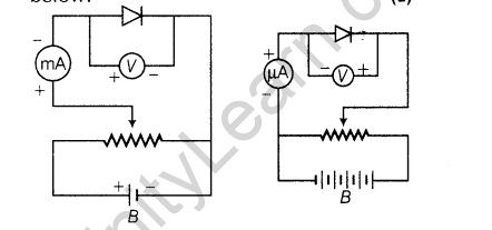
The width of depletion layer (i) decreases in forward bias.
(ii) increases in reverse bias.
23.Carbon and silicon both have four valence electrons each, then how are they distinguished? [Delhi 2011 c]
Ans.The four valence electrons of carbon are present in second orbit while that of silicon in third orbit. So, energy required to extricate an electron from silicon is much smaller than carbon.
Therefore, the number of free electrons for conduction in silicon is significant on contrary of carbon. This makes silicon conductivity much higher than carbon. This is the main distinguishable property.
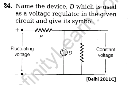
Ans.

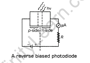
25.Draw the circuit diagram of an illuminated photo diode in reverse bias. How is photo diode used to measure light intensity? [Delhi 2010]26.Write the main use of the
(i)photo diode
(ii)Zener diode. [All India 2010 c]
Ans.Circuit diagram of illuminated photo diode in reverse bias is shown below:
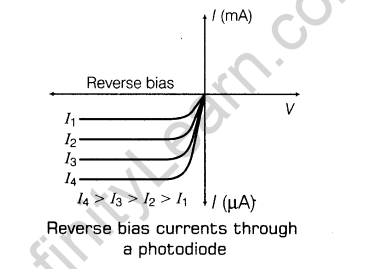
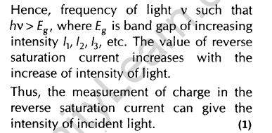
26.Write the main use of the (i) photo diode (ii) Zener diode [All India 2010 c]
Ans.Main use of photo diode In demodulation of optical signal and detection of optical signal.
Main use of Zener diode As DC voltage regulator.
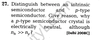
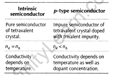
Ans.Differences between intrinsic and p-type semiconductors are given below:
In p-type semiconductor, trivalent impurity is doped with tetravalent pure semiconductor. Both type of atom (impurity and host semiconductor) are electrically neutral and hence, so produced p-type semiconductor is electrically neutral
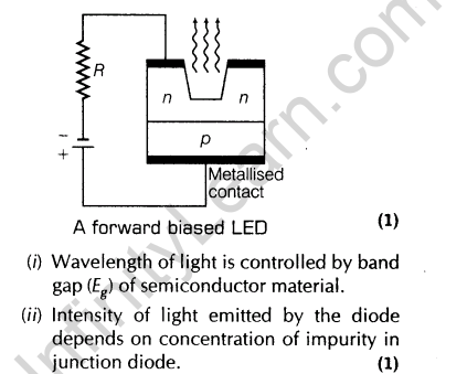
28.Draw a circuit diagram showing the biasing of an LED. State the factor which controls
(i)wavelength of light.
(ii) intensity of light emitted by the diode. [Foreign 2008]
Ans.Circuit diagram of a forward biased LED is shown below:
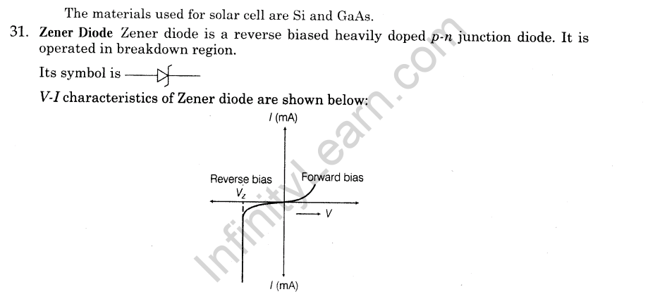
29.How is that the reverse current in a Zener diode starts increasing suddenly at a relatively low breakdowns voltage of 5 V or so?[All India 2008 C]
Ans.
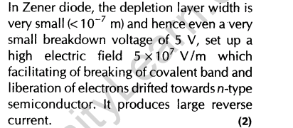
30.Draw the (i) symbol and (ii) the reverse I-V characteristics of a Zener diode. Explain briefly, which property of the characteristics enables us to use Zener diode as voltage regulator. [All India 2008 C]
Ans. Zener diode is used as voltage regulator.
Principle Zener diode is operated in the reverse breakdown region. The voltage across it remains constant, equal to the breakdown voltage for large charge in reverse current


3 Marks Questions
31.Write any two distinguishing features between conductors, semiconductors and insulators on the basis of energy band diagrams. [All India 2014]32.Draw the circuit diagram of a full-wave rectifier using p-n junction diode. Explain its working and show the output input waveforms. [Delhi 2012]
Ans.
32.Draw the circuit diagram of a full-wave rectifier using p-n junction diode. Explain its working and show the output input wave forms. [Delhi 2012]
Ans.


33.Draw V-I characteristics of a p-n junction diode. Answer the following questions, giving reasons.
(i)Why is the current under reverse bias almost independent of the applied potential up to a critical voltage?
(ii)Why does the reverse current show a sudden increase at the critical voltage?
Name any semiconductor device which operates under the reverse bias in the breakdown region.
[All India 2012]
Ans.
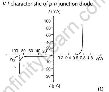
(i)Under the reverse bias condition, the holes of p-side are attracted towards the negative terminal of the battery and the electrons of the n-side are attracted towards the positive terminal of the battery. This increases the depletion layer and the potential barrier. However, the minority charge carriers are drifted across the junction producing a small current.
At any temperature, the number of minority carriers is constant, so there is the small current at any applied potential. This is the reason for the current under reverse bias to be almost’independent of applied potential. At the critical voltage, avalanche breakdown takes place which results in a sudden flow of large current.
(ii) At the critical voltage, the holes in the n-side and conduction electrons in the p-side are accelerated due to the reverse bias voltage. These minority carriers acquire sufficient kinetic energy from the electric field and collide with a valence electron.
Thus, the bond is finally broken and the valence electrons move into the conduction band resulting in enormous flow of electrons and thus, formation of hole-electron pairs. Thus, there is a sudden increase in the current at the critical voltage.
Zener diode is a semiconductor device which operates under the reverse bias in the breakdown region.
34.Draw a labelled diagram of a full -wave rectifier circuit. State its working principle. Show the input-output wave forms.[All India 2011]
Ans.


35.Name the important processes that occurs during the formation of a p-n junction.Explain briefly, with the help of asuitable diagram, how a p-n junction is formed.Define the term ‘barrier potential’?[Foreign 2011]
Ans.
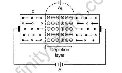
During formation of p-n junction, diffusion of charge takes place. As, soon as p-type semiconductor is joined with n-type semiconductor, diffusion of free charges across the junction starts.
For explanation of formation p-n junction
With the formation of p-n junction, the holes from p-region diffuse into the n-region and electrons from n-region diffuse into p-region and electron-hole pair combine and get annihilated.
This input produces potential barrier, VB across in junction which opposes the further diffusion through the junction. Thus, small region forms in the vicinity of the junction which is depleted of free charge carrier and has only immotile ions is called the depletion region.
Potential barrier The potential distribution near the p-n junction is known as potential barrier
36.(i) Why is a photo diode operated in reverse bias mode?
(ii)For what purpose is a photo diode used?
(iii)Draw its I-V characteristics for different intensities of illumination. [HOTS; All India 2011 C]
Ans.

(i) Photo diode is connected in reverse bias and feeble reverse current flows due to thermally generated electron-hole pair, known as dark current. When light of
(ii)Main use of photo diode In demodulation of optical signal and detection of optical signal.
(iii)Circuit diagram of illuminated photo diode in reverse bias is shown below:


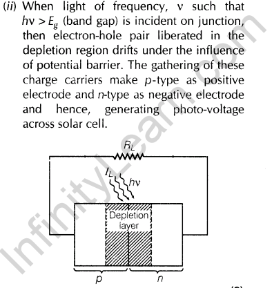
37.(i)Why are Si and GaAs preferred materials for solar cells?
(ii)Describe briefly with the help of a necessary circuit diagram, the working principle of a solar cell.[All India 2011 C]
Ans. (i) solar radiation is nearly 1.5 eV. In order to have photo excitation, the energy of radiation (hv) must be greater than energy band gap (Eg). Therefore, the semiconductor with energy band gap about 1.5 eV or lower than it and with higher absorption coefficient is likely to give better solar conversion efficiency. The energy band gap for Si is about 1.1 eV, while for GaAs, it is about 1.53 eV. The GaAs is better inspite of its higher band gap than Si because it absorbs relatively more energy from the incident solar radiations being of relatively higher absorption coefficient.
38.(i) Describe the working of Light Emitting Diodes (LEDs).
(ii)Which semiconductors are preferred to make LEDs and why?
(iii)Give two advantages of using LEDs over conventional incandescent low power lamps.[All India 2011]
Ans.(i) Working of LED LED is a forward biased p-n junction which converts electrical energy into optical energy of infrared and visible light region.
Being in forward bias, thin depletion layer and low potential barrier facilitate diffusion of electron and hole through the junction when high energy electron of conduction band combines with the low energy holes in valence band, then energy is released in the form of photon, may be seen in the form of light.
(ii) Semiconductors with appropriate band gap (Eg) close to 1.5 eV are preferred to make LED size GaAs, CdTe, etc.the other reasons to select these materials e high optical absorption, availability of raw material and low cost
(iii) Uses of LEDs (a) LED can operate at very low voltage and consumes less power in comparison to incandescent lamps
(b) Unlike the lamps, they take very less operational time and have long life.
39.With the help of a suitable diagram, explain the formation of depletion region in a p-n junction. How does its width change when the junction is
(i)forward biased and
(ii)reverse biased? [All India 2009]
Ans. With the formation of p-n junction, the holes from p-region diffuse into the n-region and electrons from n-region diffuse into p-region and electron-hole pair combine and get annihilated.
This input produces potential barrier, VB across in junction which opposes the further diffusion through the junction. Thus, small region forms in the vicinity of the junction which is depleted of free charge carrier and has only immotile ions is called the depletion region.
Circuit diagram of forward biased and reverse biased p-n junction diode is shown

The width of depletion layer (i) decreases in forward bias.
(ii) increases in reverse bias.
40.(i) With the help of circuit diagrams, distinguish between forward biasing and reverse biasing of p-n junction diode.
(ii)Draw V-I characteristics of a p-n junction diode in
(a)forward bias.
(b)reverse bias. [AH India 2009]
Ans.(i)Circuit diagram of forward biased and reverse biased p-n junction diode is shown

The width of depletion layer (a) decreases in forward bias.
(b) increases in reverse bias.
(ii)(a)Differences between forward and reverse biases are given below:

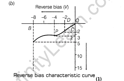
At the critical voltage, the holes in the n-side and conduction electrons in the p-side are accelerated due to the reverse bias voltage. These minority carriers acquire sufficient kinetic energy from the electric field and collide with a valence electron.
Thus, the bond is finally broken and the valence electrons move into the conduction band resulting in enormous flow of electrons and thus, formation of hole-electron pairs. Thus, there is a sudden increase in the current at the critical voltage.
Zener diode is a semiconductor device which operates under the reverse bias in the breakdown region.
41.Explain with the help of a circuit diagram how a Zener diode works as a DC voltage regulator? Draw its I-V characteristic s.[All India 2009]
Ans. Zener diode is used as voltage regulator.
Principle Zener diode is operated in the reverse breakdown region. The voltage across it remains constant, equal to the breakdown voltage for large charge in reverse current

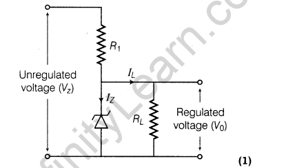
42.How is a Zener diode fabricated so as to make it a special purpose semiconductor diode? Draw the circuit diagram of a Zener diode as a voltage regulator and explain its working. [All India 2009 C]
Ans.Zener diode fabrication Zener diode is made by heavily doping of both p and n-type semiconductors and hence, the width of depletion layer becomes thin which lead to produce large electric field to increase the current even on applying reverse voltage of 4 or 5 V.
(i)Zener diode is used as voltage regulator.
Principle Zener diode is operated in the reverse breakdown region. The voltage across it remains constant, equal to the breakdown voltage for large charge in reverse current

(ii) From the figure, it is clear that the device, X is a full-wave rectifier. Circuit diagram as shown in figure below:
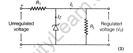
Zener diode connected with unregulated DC voltage in reverse bias. When the input voltage increases, then current through R, increase and hence, voltage drop across Rp increases while voltage across the Zener diode remains constant. The voltage across Zener diode remains constant beyond Zener voltage and hence, same/constant regulated voltage is obtained across RL.
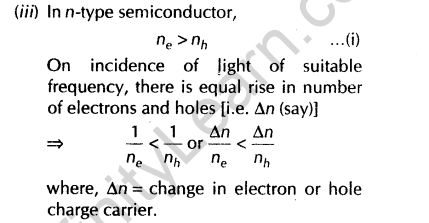
Thus, fractional change in minority charge carrier (hole) is much higher than fraction change in majority charge carrier (electron). Also, minority charge carrier contribute in drift current in reverse bias.
Thus, with incidence of light, fractional change in minority charge carrier is significant. Therefore, photo diode should be connected in reverse bias for measuring light intensity.
43.The figure below, shows the V-I characteristics of a semiconductor diode.
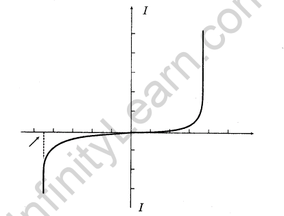
(i)Identify the semiconductor diode used.
(ii) Draw the circuit diagram to obtain the given characteristic of this device.
(iii) Briefly explain, how this diode can be used as a voltage regulator.[Delhi 2008]
Ans.(i) Zener diode
(ii) From the figure, it is clear that the device, X is a full-wave rectifier. Circuit diagram as shown in figure below:

Zener diode connected with unregulated DC voltage in reverse bias. When the input voltage increases, then current through R, increase and hence, voltage drop across Rp increases while voltage across the Zener diode remains constant. The voltage across Zener diode remains constant beyond Zener voltage and hence, same/constant regulated voltage is obtained across RL.
(iii) Zener diode is used as voltage regulator.
Principle Zener diode is operated in the reverse breakdown region. The voltage across it remains constant, equal to the breakdown voltage for large charge in reverse current

5Marks Questions
44.(i)State briefly the processes involved in the formation of p-n junction, explaining clearly how the
depletion region is formed.
(ii)Using the necessary circuit diagrams, show how the V-I characteristics of a p-n junction are obtained in (a) forward biasing (b) reverse biasing How are these characteristics made use of in rectification? [Delhi 2014]
Ans.(i) p-n Junction A p-n junction is an arrangement made by a close contact of n-type semiconductor and p-type semiconductor.There are various methods of forming p-n junction diode. In one method, an n-type germanium crystal is cut into thin slices called wafers. An aluminium film is laid on an n-type wafer which is then heated in an oven at a temperature of about 600°C. Aluminium then diffuses into the surface of wafer. In this way, a p-type semiconductor is formed on n-type semiconductor.
Formation of Depletion Region in p-n Junction In an n-type semiconductor, the concentration of electrons is more than concentration of holes. Similarly, in a p-type semiconductor, the concentration of holes is more than that of concentration of electrons. During formation of p-n junction and due to the concentration gradient across p and n-sides, holes diffuse from p-side to n-side ( p—> n) and electrons diffuse from n-side to p-side (n —> p).
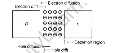
The diffused charge carriers combine with their counterparts in the immediate vicinity of the junction and neutralise each other, (l) Thus, near the junction, positive charge is built on n-side and negative charge on p-side This sets up potential difference across the junction and an internal electric field Ej directed from n-side to p-side. The equilibrium is established when the field £, becomes strong enough to stop further diffusion of the majority charge carriers (however, it helps the minority charge carriers to diffuse across the junction).The region on either side of the junction which becomes depleted (free) from the mobile charge carriers is called depletion region or depletion layer. The width of depletion region is of the order of 10-6 m.The potential difference developed across the depletion region is called the potential barrier. Potential barrier depends on dopant concentration in the semiconductor and temperature of the junction.
(ii) (a) Forward Biased Characteristics
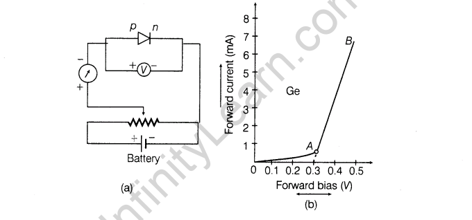
The circuit diagram for studying forward biased characteristics is shown in the figure. Starting from a low value, forward bias voltage is increased step by step (measured by voltmeter) and forward current is noted (by ammeter). A graph is plotted between voltage and current. The curve so obtained is the forward characteristic of the diode.
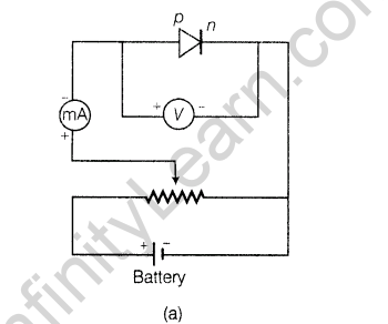
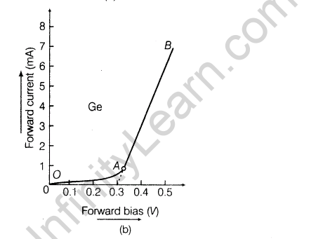
At the start when applied voltage is low, the current through the diode is almost zero. It is because of the potential barrier, which opposes the applied voltage. Till the applied voltage exceeds the potential barrier, the current increases very slowly with increase in applied voltage (OA portion of the graph).With further increase in applied voltage, the current increases very rapidly (AB portion of the graph), in this situation, the diode behaves like a conductor. The forward voltage beyond which the current through the junction starts increasing rapidly with voltage is called knee voltage. If line AB is extended back, it cuts the voltage axis at potential barrier voltage.
(b) Reverse Biased Characteristics
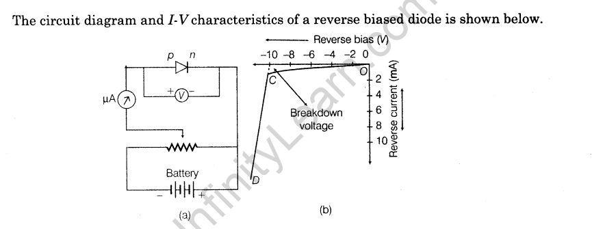
The circuit diagram for studying reverse biased characteristics is shown in the figure.
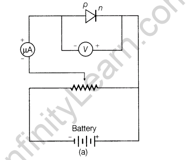
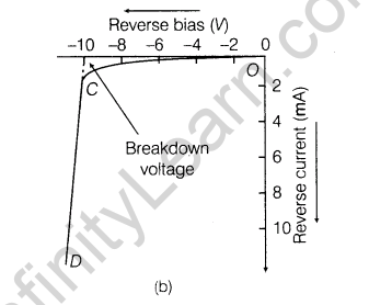
In reverse biased, the applied voltage supports the flow of minority charge carriers across the junction. So, a very small current flows across the junction due to minority charge carriers.
Motion of minority charge carriers is also supported by internal potential barrier, so all the minority carriers cross over the junction.Therefore, the small reverse current remains almost constant over a sufficiently long range of reverse bias, increasing very little with increasing voltage (OC portion of the graph). This reverse current is voltage independent upto certain voltage known as breakdown voltage and this voltage independent current – is called reverse saturation current.
Use of p-n Junction Characteristics in Rectification
From forward and reverse characteristics, it is clear that current flows through the junction diode only in forward bias not in reverse bias i.e. current flows only in one direction
45.(a) Draw the circuit arrangement for studying the V-I characteristics of a p-n junction diode in (i) forward and (ii) reverse bias. Briefly explain how the typical V- I characteristics of a diode are obtained and draw these characteristics.
(b)With the help of necessary circuit diagram, explain the working of a photo diode used for detecting optical signals. [All India 2014 C]
Ans. (a) Forward Biased Characteristics
The circuit diagram for studying forward biased characteristics is shown in the figure. Starting from a low value, forward bias voltage is increased step by step (measured by voltmeter) and forward current is noted (by ammeter). A graph is plotted between voltage and current. The curve so obtained is the forward characteristic of the diode.


At the start when applied voltage is low, the current through the diode is almost zero. It is because of the potential barrier, which opposes the applied voltage. Till the applied voltage exceeds the potential barrier, the current increases very slowly with increase in applied voltage (OA portion of the graph).With further increase in applied voltage, the current increases very rapidly (AB portion of the graph), in this situation, the diode behaves like a conductor. The forward voltage beyond which the current through the junction starts increasing rapidly with voltage is called knee voltage. If line AB is extended back, it cuts the voltage axis at potential barrier voltage.
(b) Reverse Biased Characteristics
The circuit diagram for studying reverse biased characteristics is shown in the figure.


In reverse biased, the applied voltage supports the flow of minority charge carriers across the junction. So, a very small current flows across the junction due to minority charge carriers.
Motion of minority charge carriers is also supported by internal potential barrier, so all the minority carriers cross over the junction.Therefore, the small reverse current remains almost constant over a sufficiently long range of reverse bias, increasing very little with increasing voltage (OC portion of the graph). This reverse current is voltage independent upto certain voltage known as breakdown voltage and this voltage independent current – is called reverse saturation current.
Use of p-n Junction Characteristics in Rectification
From forward and reverse characteristics, it is clear that current flows through the junction diode only in forward bias not in reverse bias i.e. current flows only in one direction
(b)Circuit diagram of illuminated photo diode in reverse bias is shown below:


46.(a) Explain with the help of diagram, how a depletion layer and barrier potential are formed in a junction diode.
(b) Draw a circuit diagram of a full-wave rectifier. Explain its working and draw input and output waveforms. [Delhi 2014 c]
Ans.(a)

During formation of p-n junction, diffusion of charge takes place. As, soon as p-type semiconductor is joined with n-type semiconductor, diffusion of free charges across the junction starts.
For explanation of formation p-n junction
With the formation of p-n junction, the holes from p-region diffuse into the n-region and electrons from n-region diffuse into p-region and electron-hole pair combine and get annihilated.
This input produces potential barrier, VB across in junction which opposes the further diffusion through the junction. Thus, small region forms in the vicinity of the junction which is depleted of free charge carrier and has only immotile ions is called the depletion region.
Potential barrier The potential distribution near the p-n junction is known as potential barrier
(b)


47.(i) How is a depletion region formed in p-n junction?
(ii)With the help of a labelled circuit diagram. Explain how a junction diode is used as a full-wave rectifier. Draw its input, output wave forms.
(iii)How do you obtain steady DC output from the pulsating voltage?[Delhi 2013 C]
Ans.(i) p-n Junction A p-n junction is an arrangement made by a close contact of n-type semiconductor and p-type semiconductor.There are various methods of forming p-n junction diode. In one method, an n-type germanium crystal is cut into thin slices called wafers. An aluminium film is laid on an n-type wafer which is then heated in an oven at a temperature of about 600°C. Aluminium then diffuses into the surface of wafer. In this way, a p-type semiconductor is formed on n-type semiconductor.
Formation of Depletion Region in p-n Junction In an n-type semiconductor, the concentration of electrons is more than concentration of holes. Similarly, in a p-type semiconductor, the concentration of holes is more than that of concentration of electrons. During formation of p-n junction and due to the concentration gradient across p and n-sides, holes diffuse from p-side to n-side ( p—> n) and electrons diffuse from n-side to p-side (n —> p).

The diffused charge carriers combine with their counterparts in the immediate vicinity of the junction and neutralise each other, (l) Thus, near the junction, positive charge is built on n-side and negative charge on p-side This sets up potential difference across the junction and an internal electric field Ej directed from n-side to p-side. The equilibrium is established when the field £, becomes strong enough to stop further diffusion of the majority charge carriers (however, it helps the minority charge carriers to diffuse across the junction).The region on either side of the junction which becomes depleted (free) from the mobile charge carriers is called depletion region or depletion layer. The width of depletion region is of the order of 10-6 m.The potential difference developed across the depletion region is called the potential barrier. Potential barrier depends on dopant concentration in the semiconductor and temperature of the junction.
(ii)


(iii) A full-wave bridge rectifier using four diodes (full-wave bridge rectifier) gives a continuous, unidirectional but pulsating output voltage or current.
The rectified output is passed through a filter circuit which removes the ripple and an almost steady DC voltage (or current) is obtained.
48.Why is a Zener diode considered as a special purpose semiconductor diode? Draw the I-V characteristics of Zener diode and explain briefly, how reverse current suddenly increase at the breakdown voltage? Describe briefly with the help of a circuit diagram, how a Zener diode work’s to obtain a constant DC voltage from the unregulated DC output of a rectifier.[Delhi 2009 C; Foreign 2012]
Ans.Zener diode works only in reverse breakdown region that is why it is considered as a special purpose semiconductor
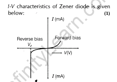
Reverse current is due to the flow of electrons from n —> p and holes from p —» n. As, the reverse biased voltage increase the elecHic field across the junction, increases signiffcantly and when reverse bias voltage V – Vz, then the electric field strength is high enough to pull the electrons from p-side and accelerated it to n-side.
These electrons are responsible for the high current at the breakdown.
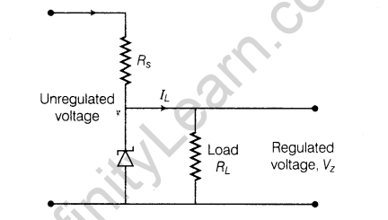
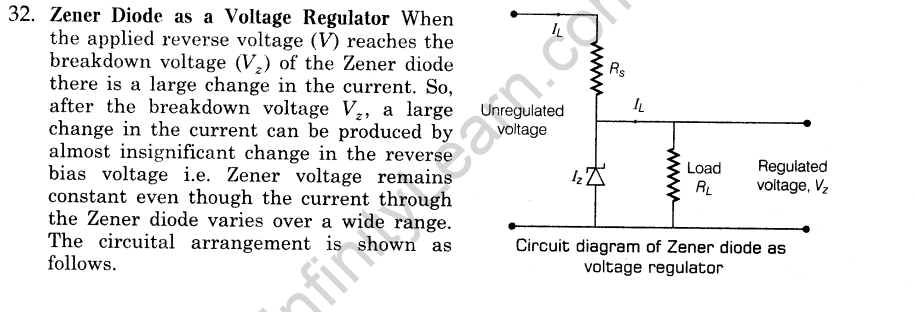
Voltage regulator converts an unregulated DC output of rectifier into a constant regulated DC voltage, using Zener diode. The unregulated voltage is connected to the Zener diode through a series resistance Rs such that the Zener diode is reverse biased. If the input voltage increases, then current through Rs apd Zener diode increases. Thus, the voltage drop across R^ increases without any change in the voltage drop across Zener diode. This is because of the breakdown region, Zener voltage remain constant even though the current through Zener diode changes.
Similarly, if the input voltage decreases, the current through Rs and Zener diode decreases. The voltage drop across Rs, decreases without any change in the voltage across the Zener diode.
Now, any change in input voltage results the change in voltage drop across Rs, without any change in voltage across the Zener diode. Thus, Zener diode acts as a voltage regulator
49.(i) Describe briefly, with the help of a diagram, the role of the two important processes involved in the formation of a p-n junction.
(ii) Name the device which is used as a voltage regulator. Draw the necessary circuit diagram and explain its working.[HOTS; All India 2012]
Ans.

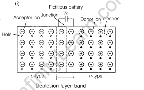
The two process involved in the formation of p-n junction.
(a)Diffusion
(b)Drift
Holes and electrons diffuse from p to n and n to p respectively.
The majority charge carrier drifts under the influence of applied electric field such that
(a)holes along applied E and
(b)electron opposite to E.
(ii) Zener diode is used as voltage regulator.
Principle Zener diode is operated in the reverse breakdown region. The voltage across it remains constant, equal to the breakdown voltage for large charge in reverse current


50.(i) Draw the circuit diagram of a p-n junction diode in
(a)forward bias.
(b)reverse bias.
How are these circuits used to study the V-1 characteristics of a silicon diode? Draw the typical V-I characteristics.
(ii) What is a Light Emitting Diode (LED)? Mention two important advantage of LEDs over conventional lamps.[Delhi 2010 C; All India 2010]
Ans.(i) p-n Junction A p-n junction is an arrangement made by a close contact of n-type semiconductor and p-type semiconductor.There are various methods of forming p-n junction diode. In one method, an n-type germanium crystal is cut into thin slices called wafers. An aluminium film is laid on an n-type wafer which is then heated in an oven at a temperature of about 600°C. Aluminium then diffuses into the surface of wafer. In this way, a p-type semiconductor is formed on n-type semiconductor.
Formation of Depletion Region in p-n Junction In an n-type semiconductor, the concentration of electrons is more than concentration of holes. Similarly, in a p-type semiconductor, the concentration of holes is more than that of concentration of electrons. During formation of p-n junction and due to the concentration gradient across p and n-sides, holes diffuse from p-side to n-side ( p—> n) and electrons diffuse from n-side to p-side (n —> p).

The diffused charge carriers combine with their counterparts in the immediate vicinity of the junction and neutralise each other, (l) Thus, near the junction, positive charge is built on n-side and negative charge on p-side This sets up potential difference across the junction and an internal electric field Ej directed from n-side to p-side. The equilibrium is established when the field £, becomes strong enough to stop further diffusion of the majority charge carriers (however, it helps the minority charge carriers to diffuse across the junction).The region on either side of the junction which becomes depleted (free) from the mobile charge carriers is called depletion region or depletion layer. The width of depletion region is of the order of 10-6 m.The potential difference developed across the depletion region is called the potential barrier. Potential barrier depends on dopant concentration in the semiconductor and temperature of the junction.
(a) Forward Biased Characteristics
The circuit diagram for studying forward biased characteristics is shown in the figure. Starting from a low value, forward bias voltage is increased step by step (measured by voltmeter) and forward current is noted (by ammeter). A graph is plotted between voltage and current. The curve so obtained is the forward characteristic of the diode.


At the start when applied voltage is low, the current through the diode is almost zero. It is because of the potential barrier, which opposes the applied voltage. Till the applied voltage exceeds the potential barrier, the current increases very slowly with increase in applied voltage (OA portion of the graph).With further increase in applied voltage, the current increases very rapidly (AB portion of the graph), in this situation, the diode behaves like a conductor. The forward voltage beyond which the current through the junction starts increasing rapidly with voltage is called knee voltage. If line AB is extended back, it cuts the voltage axis at potential barrier voltage.
(b) Reverse Biased Characteristics
The circuit diagram for studying reverse biased characteristics is shown in the figure.


In reverse biased, the applied voltage supports the flow of minority charge carriers across the junction. So, a very small current flows across the junction due to minority charge carriers.
Motion of minority charge carriers is also supported by internal potential barrier, so all the minority carriers cross over the junction.Therefore, the small reverse current remains almost constant over a sufficiently long range of reverse bias, increasing very little with increasing voltage (OC portion of the graph). This reverse current is voltage independent upto certain voltage known as breakdown voltage and this voltage independent current – is called reverse saturation current.
Use of p-n Junction Characteristics in Rectification
From forward and reverse characteristics, it is clear that current flows through the junction diode only in forward bias not in reverse bias i.e. current flows only in one direction
(ii) (a) Working of LED LED is a forward biased p-n junction which converts electrical energy into optical energy of infrared and visible light region.
Being in forward bias, thin depletion layer and low potential barrier facilitate diffusion of electron and hole through the junction when high energy electron of conduction band combines with the low energy holes in valence band, then energy is released in the form of photon, may be seen in the form of light.
(b)Uses of LEDs (a) LED can operate at very low voltage and consumes less power in comparison to incandescent lamps. Unlike the lamps, they take very less operational time and have long life.
51.(i) Draw I-V characteristics of a Zener diode.
(ii)Explain with the help of a circuit diagram, the use of a Zener diode as a voltage regulator.
(iii)A photo diode is operated under reverse bias although in the forward bias, the current is known to be more than the current in the reverse bias. Explain, giving reason. [HOTS; Foreign 2010]
Ans. (i)Zener diode is used as voltage regulator.
Principle Zener diode is operated in the reverse breakdown region. The voltage across it remains constant, equal to the breakdown voltage for large charge in reverse current

(ii) From the figure, it is clear that the device, X is a full-wave rectifier. Circuit diagram as shown in figure below:

Zener diode connected with unregulated DC voltage in reverse bias. When the input voltage increases, then current through R, increase and hence, voltage drop across Rp increases while voltage across the Zener diode remains constant. The voltage across Zener diode remains constant beyond Zener voltage and hence, same/constant regulated voltage is obtained across RL.

Thus, fractional change in minority charge carrier (hole) is much higher than fraction change in majority charge carrier (electron). Also, minority charge carrier contribute in drift current in reverse bias.
Thus, with incidence of light, fractional change in minority charge carrier is significant. Therefore, photo diode should be connected in reverse bias for measuring light intensity.
52.(i) Draw a circuit arrangement for studying V-I characteristics of a p-n junction diode in(a)forward bias and (b) reverse bias.
Show typical V-I characteristics of a silicon diode.
(ii) State the main practical application of LED. Explain, giving reason, why the semiconductor used for
fabrication of visible light LEDs must have a band gap of at least (nearly) 1.8 eV. [Delhi 2010 C]
Ans.(i) p-n Junction A p-n junction is an arrangement made by a close contact of n-type semiconductor and p-type semiconductor.There are various methods of forming p-n junction diode. In one method, an n-type germanium crystal is cut into thin slices called wafers. An aluminium film is laid on an n-type wafer which is then heated in an oven at a temperature of about 600°C. Aluminium then diffuses into the surface of wafer. In this way, a p-type semiconductor is formed on n-type semiconductor.
Formation of Depletion Region in p-n Junction In an n-type semiconductor, the concentration of electrons is more than concentration of holes. Similarly, in a p-type semiconductor, the concentration of holes is more than that of concentration of electrons. During formation of p-n junction and due to the concentration gradient across p and n-sides, holes diffuse from p-side to n-side ( p—> n) and electrons diffuse from n-side to p-side (n —> p).

The diffused charge carriers combine with their counterparts in the immediate vicinity of the junction and neutralise each other, (l) Thus, near the junction, positive charge is built on n-side and negative charge on p-side This sets up potential difference across the junction and an internal electric field Ej directed from n-side to p-side. The equilibrium is established when the field £, becomes strong enough to stop further diffusion of the majority charge carriers (however, it helps the minority charge carriers to diffuse across the junction).The region on either side of the junction which becomes depleted (free) from the mobile charge carriers is called depletion region or depletion layer. The width of depletion region is of the order of 10-6 m.The potential difference developed across the depletion region is called the potential barrier. Potential barrier depends on dopant concentration in the semiconductor and temperature of the junction.
(a) Forward Biased Characteristics
The circuit diagram for studying forward biased characteristics is shown in the figure. Starting from a low value, forward bias voltage is increased step by step (measured by voltmeter) and forward current is noted (by ammeter). A graph is plotted between voltage and current. The curve so obtained is the forward characteristic of the diode.


At the start when applied voltage is low, the current through the diode is almost zero. It is because of the potential barrier, which opposes the applied voltage. Till the applied voltage exceeds the potential barrier, the current increases very slowly with increase in applied voltage (OA portion of the graph).With further increase in applied voltage, the current increases very rapidly (AB portion of the graph), in this situation, the diode behaves like a conductor. The forward voltage beyond which the current through the junction starts increasing rapidly with voltage is called knee voltage. If line AB is extended back, it cuts the voltage axis at potential barrier voltage.
(b) Reverse Biased Characteristics
The circuit diagram for studying reverse biased characteristics is shown in the figure.


In reverse biased, the applied voltage supports the flow of minority charge carriers across the junction. So, a very small current flows across the junction due to minority charge carriers.
Motion of minority charge carriers is also supported by internal potential barrier, so all the minority carriers cross over the junction.Therefore, the small reverse current remains almost constant over a sufficiently long range of reverse bias, increasing very little with increasing voltage (OC portion of the graph). This reverse current is voltage independent upto certain voltage known as breakdown voltage and this voltage independent current – is called reverse saturation current.
Use of p-n Junction Characteristics in Rectification
From forward and reverse characteristics, it is clear that current flows through the junction diode only in forward bias not in reverse bias i.e. current flows only in one direction
(ii) Working of LED LED is a forward biased p-n junction which converts electrical energy into optical energy of infrared and visible light region.
Being in forward bias, thin depletion layer and low potential barrier facilitate diffusion of electron and hole through the junction when high energy electron of conduction band combines with the low energy holes in valence band, then energy is released in the form of photon, may be seen in the form of light.
(a) Semiconductors with appropriate band gap (Eg) close to 1.5 eV are preferred to make LED size GaAs, CdTe, etc.the other reasons to select these materials e high optical absorption, availability of raw material and low cost
(b) Uses of LEDs
(i) LED can operate at very low voltage and consumes less power in comparison to incandescent lamps
(ii) Unlike the lamps, they take very less operational time and have long life.
53.How is a Zener diode fabricated so as to make it a special purpose diode? Draw 7-V characteristics of Zener diode and explain the significance of breakdown voltage, (ii) Explain briefly, with the help of a circuit diagram, how a p-n junction diode works as a half-wave rectifier. [Delhi 2009c]
Ans.(i)Zener diode works only in reverse breakdown region that is why it is considered as a special purpose semiconductor

Reverse current is due to the flow of electrons from n —> p and holes from p —» n. As, the reverse biased voltage increase the elecHic field across the junction, increases signiffcantly and when reverse bias voltage V – Vz, then the electric field strength is high enough to pull the electrons from p-side and accelerated it to n-side.
These electrons are responsible for the high current at the breakdown.

Voltage regulator converts an unregulated DC output of rectifier into a constant regulated DC voltage, using Zener diode. The unregulated voltage is connected to the Zener diode through a series resistance Rs such that the Zener diode is reverse biased. If the input voltage increases, then current through Rs apd Zener diode increases. Thus, the voltage drop across R^ increases without any change in the voltage drop across Zener diode. This is because of the breakdown region, Zener voltage remain constant even though the current through Zener diode changes.
Similarly, if the input voltage decreases, the current through Rs and Zener diode decreases. The voltage drop across Rs, decreases without any change in the voltage across the Zener diode.
Now, any change in input voltage results the change in voltage drop across Rs, without any change in voltage across the Zener diode. Thus, Zener diode acts as a voltage regulator
(ii) Circuit diagram of p-n junction diode as half-wave rectifier is shown below
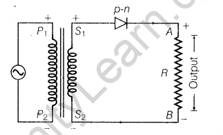
Diode conducts corresponding to positive half cycle and does not conduct during negative half cycle hence, AC is converted by diode into unidirectional pulsating DC. This action is known as half-wave rectification.
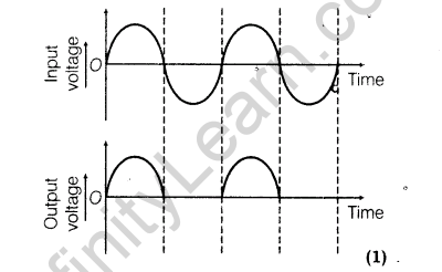
54.(i) Draw the typical shape of the V-I characteristics of a p-n junction diode both in (a) forward(b)reverse bias configuration. How do we infer, from these characteristics that a diode can be used to rectify alternating voltages?
(ii) Draw the circuit diagram of a full-wave rectifier using a centre-tap transformer and two p-n junction diodes. Give a brief description of the working of this circuit. [Delhi 2009 C]
Ans.(i) p-n Junction A p-n junction is an arrangement made by a close contact of n-type semiconductor and p-type semiconductor.There are various methods of forming p-n junction diode. In one method, an n-type germanium crystal is cut into thin slices called wafers. An aluminium film is laid on an n-type wafer which is then heated in an oven at a temperature of about 600°C. Aluminium then diffuses into the surface of wafer. In this way, a p-type semiconductor is formed on n-type semiconductor.
Formation of Depletion Region in p-n Junction In an n-type semiconductor, the concentration of electrons is more than concentration of holes. Similarly, in a p-type semiconductor, the concentration of holes is more than that of concentration of electrons. During formation of p-n junction and due to the concentration gradient across p and n-sides, holes diffuse from p-side to n-side ( p—> n) and electrons diffuse from n-side to p-side (n —> p).

The diffused charge carriers combine with their counterparts in the immediate vicinity of the junction and neutralise each other, (l) Thus, near the junction, positive charge is built on n-side and negative charge on p-side This sets up potential difference across the junction and an internal electric field Ej directed from n-side to p-side. The equilibrium is established when the field £, becomes strong enough to stop further diffusion of the majority charge carriers (however, it helps the minority charge carriers to diffuse across the junction).The region on either side of the junction which becomes depleted (free) from the mobile charge carriers is called depletion region or depletion layer. The width of depletion region is of the order of 10-6 m.The potential difference developed across the depletion region is called the potential barrier. Potential barrier depends on dopant concentration in the semiconductor and temperature of the junction.
(a) Forward Biased Characteristics
The circuit diagram for studying forward biased characteristics is shown in the figure. Starting from a low value, forward bias voltage is increased step by step (measured by voltmeter) and forward current is noted (by ammeter). A graph is plotted between voltage and current. The curve so obtained is the forward characteristic of the diode.


At the start when applied voltage is low, the current through the diode is almost zero. It is because of the potential barrier, which opposes the applied voltage. Till the applied voltage exceeds the potential barrier, the current increases very slowly with increase in applied voltage (OA portion of the graph).With further increase in applied voltage, the current increases very rapidly (AB portion of the graph), in this situation, the diode behaves like a conductor. The forward voltage beyond which the current through the junction starts increasing rapidly with voltage is called knee voltage. If line AB is extended back, it cuts the voltage axis at potential barrier voltage.
(b) Reverse Biased Characteristics
The circuit diagram for studying reverse biased characteristics is shown in the figure.


In reverse biased, the applied voltage supports the flow of minority charge carriers across the junction. So, a very small current flows across the junction due to minority charge carriers.
Motion of minority charge carriers is also supported by internal potential barrier, so all the minority carriers cross over the junction.Therefore, the small reverse current remains almost constant over a sufficiently long range of reverse bias, increasing very little with increasing voltage (OC portion of the graph). This reverse current is voltage independent upto certain voltage known as breakdown voltage and this voltage independent current – is called reverse saturation current.
Use of p-n Junction Characteristics in Rectification
From forward and reverse characteristics, it is clear that current flows through the junction diode only in forward bias not in reverse bias i.e. current flows only in one direction
(ii)

