To draw I-V characteristic curve: When a p-n junction is in forward bias, current flows through the junction from the p-side to the n-side. The forward bias voltage creates a potential difference across the junction, which allows electrons to flow from the n-side to the p-side. The net result is a small current flowing through the junction.
When a p-n junction is in reverse bias, current does not flow through the junction. The reverse bias voltage creates a potential difference across the junction, which prevents electrons from flowing from the n-side to the p-side. The net result is no current flowing through the junction.
In this article, let us learn how to draw the I-V characteristic curve of a p-n junction in forward bias and reverse bias.
To draw the I-V characteristic curve of a p-n junction in forward bias and reverse bias
Aim
To draw the I-V characteristic curve of a p-n junction in forward bias and reverse bias.
Apparatus
A p-n junction (semi-conductor) diode, a 3 volt battery, a 50 volt battery, a high resistance rheostat, one 0-3 volt voltmeter, one 0-50 volt voltmeter, one 0-100 mA ammeter, one 0-100 μA ammeter, one way key, connecting wires and pieces of sand paper.
Theory
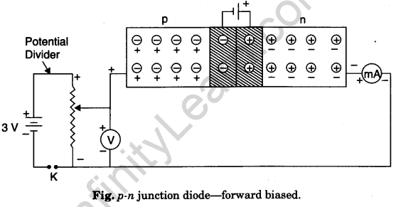
Forward bias characteristics. When the p -section of the diode is connected to positive terminal of a battery and n-section is connected to negative terminal of the battery then junction is said to be forward biased. With increase in bias voltage, the forward current increases slowly in the beginning and then rapidly. At about 0.7 V for Si diode (0.2 V for Ge), the current increases suddenly. The value of forward bias voltage, at which the forward current increases rapidly, is called cut in voltage or threshold voltage.
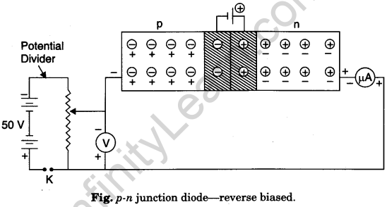
Reverse bias characteristics. When the p -section of the diode is connected to negative terminal of high voltage battery and n-section of the diode is connected to positive terminal of the same battery, then junction is said to be reverse biased.
When reverse bias voltage increases, initially there is a very small reverse current flow, which remains almost constant with bias. But when reverse bias voltage increases to sufficiently high value, the reverse current suddenly increases to a large value. This voltage at which breakdown of junction diode occurs (suddenly large current flow) is called zener breakdown voltage or inverse voltage. The breakdown voltage may^tarts from one volt to several hundred volts, depending upon dopant density and the depletion layer.
Diagram
Procedure
For forward-bias
- Make circuit diagram as shown in diagram.
- Make all connections neat, clean and tight.
- Note least count and zero error of voltmeter (V) and milli-ammeter (mA).
- Bring moving contact of potential divider (rheostat) near negative end and insert the key K. Voltmeter V and milli-ammeter mA will give zero reading.
- Move the contact a little towards positive end to apply a forward-bias voltage (VF) of
0. 1 V. Current remains zero. - Increase the forward-bias voltage upto 0.3 V for Ge diode. Current remains zero, (It is due to junction potential barrier of 0.3 V).
- Increase VF to 0.4 V. Milli-ammeter records a small current.
- Increase VF in steps of 0.2 V and note the corresponding current. Current increases first slowly and then rapidly, till VF becomes 0.7 V.
- Make VF = 0.72 V. The current increases suddenly. This represents “forward break-down” stage.
- If the VF increases beyond “forward breakdown” stage, the forward current does not change much. Now take out the key at once.
- Record your observations as given ahead.
For reverse-bias - Make circuit diagram as shown in diagram.
- Make all connections neat, clean and tight.
- Note least count and zero error of voltmeter (V) and micro-ammeter (μA).
- Bring moving contact of potential divider (rheostat) near positive end and insert the key K Voltmeter V and micro-ammeter μA will give zero reading.
- Move the contact towards negative end to apply a reverse-bias voltage (VR) of 0.5 V, a feebly reverse current starts flowing.
- Increase VR in steps of 0.2 V. Current increases first slowly and then rapidly till VR becomes 20 V. Note the current.
- Make VR = 25 V. The current increases suddenly. This represents “reverse break-down” stage. Note the current and take out the key at once.
- Record your observations as given ahead.
Observations
For forward-bias
Range of voltmeter = …..V
Least count of voltmeter = …..V
Zero error of voltmeter = …..V
Range of milli-ammeter = …..mA
Least count of milli-ammeter = …..mA
Zero error of milli-ammeter = …..mA
1. Table for forward-bias voltage and forward current
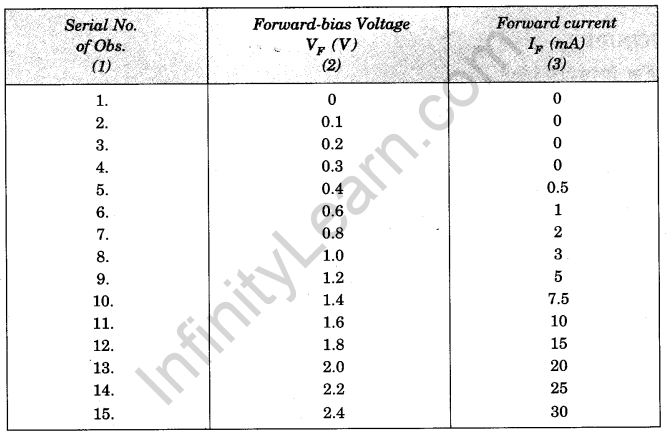
Note. The readings are as a sample.
For reverse-bias
Range of voltmeter = …..V
Least count of voltmeter = …..V
Zero error of voltmeter = …..V
Range of micro-ammeter = …..μA
Least count of micro-ammeter = …..μA
Zero error of micro-ammeter = …..
2. Table for reverse-bias voltage and reverse current
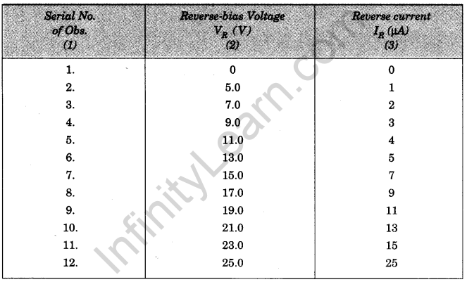
Note. The readings are given as a sample.
Calculations
For forward-bias
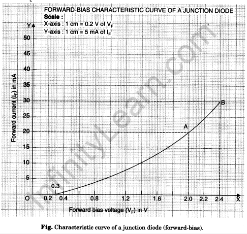
Plot a graph between forward-bias voltage VF (column 2) and forward current IF (column 3) taking VF along X-axis and IF along Y-axis.
This graph is called forward-bias characteristic curve a junction diode.

For reverse-bias
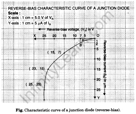
Plot a graph between reverse-bias voltage VR (column 2) and reverse current IR (column 3) taking VR along X-axis and IR along Y-axis.
This graph is called reverse-bias characteristic curve of a junction diode.

Result
Junction resistance for forward-bias = 40 ohms
Junction resistance for reverse-bias = 2 x 10⁶ ohms.
Precautions
- All connections should be neat, clean and tight.
- Key should be used in circuit and opened when the circuit is not being used.
- Forward-bias voltage beyond breakdown should not be applied.
- Reverse-bias voltage beyond breakdown should not be applied.
Sources of error
The junction diode supplied may be faulty.
Viva Voce – To draw the I-V characteristic curve of a p-n junction
Question. 1. Define energy level in an atom.
Answer. Definite energy value of an electron in the subshell of the atom, is called energy level of the atom.
Question. 2. Define energy band in a crystal.
Answer. Broadened energy level (line) in a crystal, is called energy band of the crystal.
Question. 3. Name different types of energy bands.
Answer. Different energy bands are :
1. Conduction band (C), 2. Valence band (V), 3. Forbidden band (F).
Question. 4. Define different energy bands.
Answer. Read Art. 10.03 (1, 2, 3, 4).
Question.5. Name different types of substances.
Answer. Different types of substances are :
1. Conductors, 2. Insulators, 3. Semiconductors.
Question. 6. Distinguish between a conductor, an insulator and a semiconductor.
Answer. Read Art. 10.04 (1, 2, 3).
Question.7. How are electrical conductivity and resistivity related?
Answer. Electrical conductivity is reciprocal of resistivity
![]()
Question. 8. What is S.I. unit of conductance?
Answer. S.I. unit of conductance is siemen (S).
Question. 9. What is order of conductivity of conductors, semiconductors and insulators?
Answer.102-108, 105-10-6 and 10-11-10-19 S m-1 respectively.
Question. 10. Define a hole.
Answer. A place vacated by an electron, is called a hole. It is associated with a positive charge.
Question.11. Define an intrinsic semiconductor.
Answer. A pure semiconductor material, is called an intrinsic semiconductor, it ne = nn
Question. 12. Which materials are commonly used as semiconductors?
Answer. Silicon and germanium are commonly used as semiconductors.
Question. 13. Which of the upper two materials has less energy gap?
Answer. Energy gap has value 0.72 eV for germanium and 1.12 eV for silicon.
Question.14. Define an extrinsic semiconductor.
Answer. A semiconductor material made deliberately impure, is called an extrinsic semiconductor.
Question.15. Describe an n-type semiconductor (Ge).
Answer. An n-type Ge is obtained by adding a small quantity (one millionth part) of a pentavalent impurity to its crystal.
Question.16. Name the pentavalent impurities which make Ge n-type.
Answer. The pentavalent impurities are :
1. Phosphorus (15), 2. Arsenic (33), 3. Antimony (51), 4. Bismuth (83).
Generally, Arsenic (As) is taken for this purpose.
Question.17. Describe a p-type semiconductor (Ge).
Answer. A p-type Ge’ is obtained by adding a small quantity (one millionth part) of a trivalent impurity to its crystal.
Question.18. Name the trivalent impurities which make Ge p-type.
Answer. The trivalent impurities are :
1. Boron (5), 2. Aluminium (13), 3. Gallium (31), 4. Indium (49), 5. Thalium (81).
Generally Indium (In) is taken for this purpose.
Question.19. What is doping?
Answer. The process of adding a suitable impurity to pure semiconductor, deliberately, is called
doping.
Question.20. What is order of doping in an extrinsic semiconductor?
Answer. It is one part in one million.
Question.21. Why is n-type semiconductor so called?
Answer. Because it contains free electrons with negative charge, as charge carriers.
Question.22. Why is p-type semiconductor so called?
Answer. Because it contains holes with positive charge, as charge carriers.
Question. 23. What is a junction?
Answer. It is a common surface of n-type and p-type semiconductor.
Question.24. What is a depletion layer?
Answer. It is a layer with junction in the middle, having no free charge carriers. The opposite j charge carriers have become neutralized. (It is shown shaded in Fig. 10.02).
Question.25. What is junction potential barrier?
Answer. The potential difference between junction ends of the two types of semiconductors, is
called junction potential barrier.
Question.26. Why is junction potential barrier so called?
Answer. Because it prevents free charge carriers from entering the depletion layer by themselves.
Question.27. What is biasing of a junction?
Answer. Applying an external potential difference more than potential barrier on the faces of the junction, is called biasing of the junction.
Question.28. Give names of the two types of the biasing.
Answer. The two types of biasing are :
(i) forward biasing (ii) reverse biasing.
Question.29. Why is forward bias so called?
Answer. Because it makes free charge carriers to move forward towards junction.
Question.30. Why is reverse bias so called?
Answer. Because it makes free charge carriers to move reverse away from junction.
Question.31. How does the bias effect the thickness of the depletion layer?
Answer. Forward bias decreases the thickness of depletion layer.
Reverse bias increases the thickness of depletion layer.
Question.32. How does the bias effect the junction resistance?
Answer. The forward bias makes junction resistance less.
The reverse bias makes junction resistance more.
Question.33. Define characteristic of a junction diode.
Answer. Graph drawn between bias voltage and circuit current of a junction diode, is called characteristic of the diode. It reveals the character (way of behaviour) of the junction diode.
Question.34. Describe different types of characteristics of a junction diode.
Answer.
- Forward bias characteristic. It is obtained by plotting a graph between forward bias
voltage and circuit current. Junction resistance comes to be about 10 ohm. - Reverse bias characteristic. It is obtained by plotting a graph between reverse bias voltage and circuit current. Junction resistance comes to be about 10,000 ohms.


